Photodiode and manufacturing method thereof

A photodiode and diode technology, applied in circuits, electrical components, semiconductor devices, etc., can solve the problems of energy loss, high polarization sensitivity, long absorption length, etc., and achieve the effect of reducing energy loss

Active Publication Date: 2013-02-06
HUAWEI TECH CO LTD +1
View PDF3 Cites 11 Cited by
  • Summary
  • Abstract
  • Description
  • Claims
  • Application Information

AI Technical Summary

Problems solved by technology

[0003] But in the existing technology, on the one hand, due to the gradual structure of the incident waveguide covered by the front end of the optical matching layer and the front end of the optical matching layer, as well as the scattering loss of the waveguide side wall and the absorption loss of the carrier, the light in the structure A considerable part of energy will be lost; on the other hand, due to the high polarization sensitivity in the optical coupling process, the coupling absorption efficiency of light at the back end of the optical matching layer and the coupling part of the avalanche photodiode is not high, and the absorption length is longer

Method used


Image

  • Photodiode and manufacturing method thereof
  • Photodiode and manufacturing method thereof
  • Photodiode and manufacturing method thereof

Examples


Embodiment Construction

[0059] The following will clearly and completely describe the technical solutions in the embodiments of the present invention with reference to the accompanying drawings in the embodiments of the present invention. Obviously, the described embodiments are only some, not all, embodiments of the present invention. Based on the embodiments of the present invention, all other embodiments obtained by persons of ordinary skill in the art without making creative efforts belong to the protection scope of the present invention.

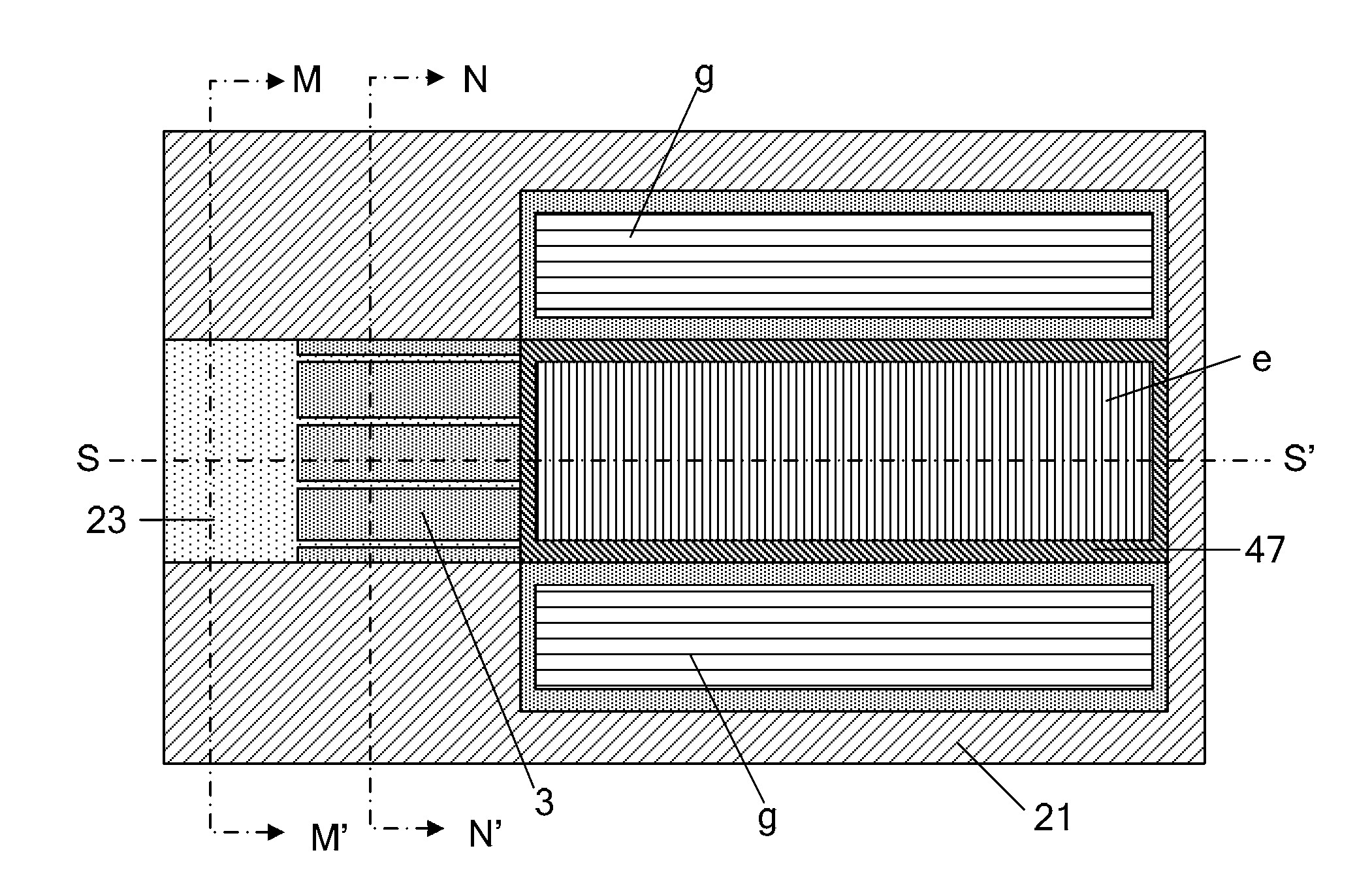
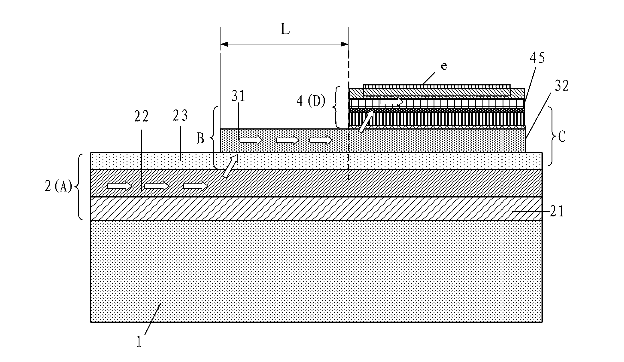
[0060] Embodiments of the present invention disclose a photodiode, such as figure 1 , 2 As shown, it includes: a substrate 1 , an incident waveguide 2 , an optical matching layer 3 and an avalanche photodiode 4 .

[0061] The incident waveguide 2 includes: a lower cladding layer 21 , an incident waveguide core layer 22 and an upper cladding layer 23 .

[0062] The lower cladding layer 21 covers the substrate 1, and the lower cladding layer 21 includes an elo...


PUM


Abstract

The embodiment of the invention discloses a photodiode and a manufacturing method thereof, relating to the field of opto-electrical technology, wherein the photodiode is capable of reducing the energy loss. The photodiode comprises a substrate positioned on a bottom layer, a lower cladding layer boss covering the substrate, an incident wave core guiding layer covering the lower cladding layer boss, an upper cladding layer covering the incident wave core guiding layer, an optical matching layer positioned above the upper cladding layer and an avalanche photodiode positioned above the middle part of the back end of the optical matching layer, wherein the width of the lower cladding layer boss at the tail end in the incident wave direction is wider than that of the beginning end in the incident wave direction, both sides of the lower cladding layer boss at the tail end in the incident wave direction are parallel, and both sides of the lower cladding layer boss at the beginning end in the incident wave direction are parallel; and the optical matching layer comprises an optical matching layer front end and an optical matching layer back end, wherein the optical matching layer front end comprises at least one air seam extended along the incident wave direction, and the optical matching layer front end is divided into characteristic units partitioned by the air seams. The embodiment of the invention is applied to manufacturing the photodiode.

Description

technical field [0001] The invention relates to the field of optoelectronic technology, in particular to a photodiode and a manufacturing method thereof. Background technique [0002] With the rapid development of optoelectronic integration technology, the demand for high-speed and high-sensitivity photodetectors that can be monolithically integrated is becoming more and more urgent. In the wave-coupled photodetector, the polarization state of the incident signal light is random, and polarization insensitivity is a general requirement of the detector, so a polarization-insensitive high-speed, high-quantum-efficiency evanescent wave-coupled avalanche photodiode is designed becomes particularly important. The optical coupling and absorption process of the evanescent wave coupling avalanche photodiode (APD) is: the first step, the light is coupled from the fiber waveguide to the optical matching layer; the second step, when the light passes through the optical matching layer w...

Claims


Application Information

Patent Timeline
Patent Type & Authority Applications(China)
IPC IPC(8): H01L31/107H01L31/0232H01L31/18
Inventor 史翠华余长亮付生猛赵彦立
Owner HUAWEI TECH CO LTD
Why Eureka
Try Eureka