Process integration of a single chip three axis magnetic field sensor

A magnetic field sensor, magnetic field component technology, applied in the direction of the magnetic field control resistor, the size/direction of the magnetic field, the components of the electromagnetic equipment, etc., can solve the problems of chip-level packaging difficulties, large vertical expansion, and high cost

Active Publication Date: 2013-02-06
EVERSPIN TECHNOLOGIES
View PDF9 Cites 45 Cited by
  • Summary
  • Abstract
  • Description
  • Claims
  • Application Information

AI Technical Summary

Problems solved by technology

Since the size of vertically bonded chips is generally dictated by the pad pitch determined by handling constraints, this technique results in a large vertical s

Method used


Image

  • Process integration of a single chip three axis magnetic field sensor
  • Process integration of a single chip three axis magnetic field sensor
  • Process integration of a single chip three axis magnetic field sensor

Examples


Embodiment Construction

[0017] The following detailed description is merely exemplary in nature and is not intended to limit the invention or the application and uses of the invention. Furthermore, there is no intention to be bound by any theory presented in the preceding background or the following detailed description.

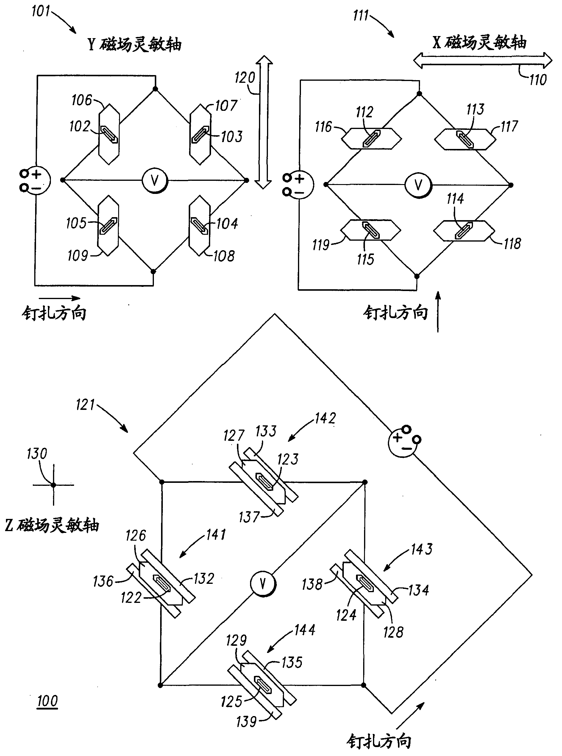
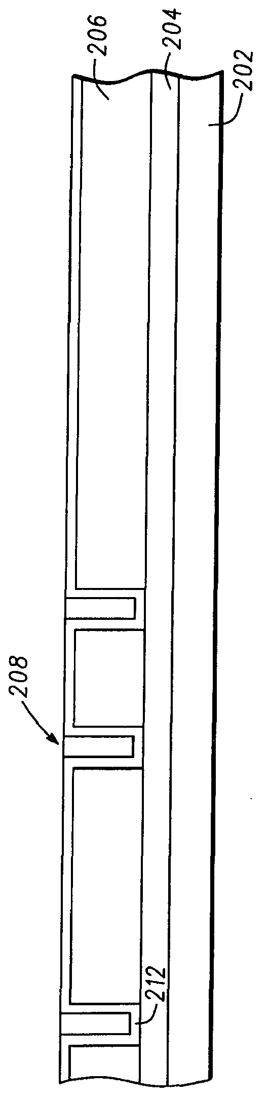
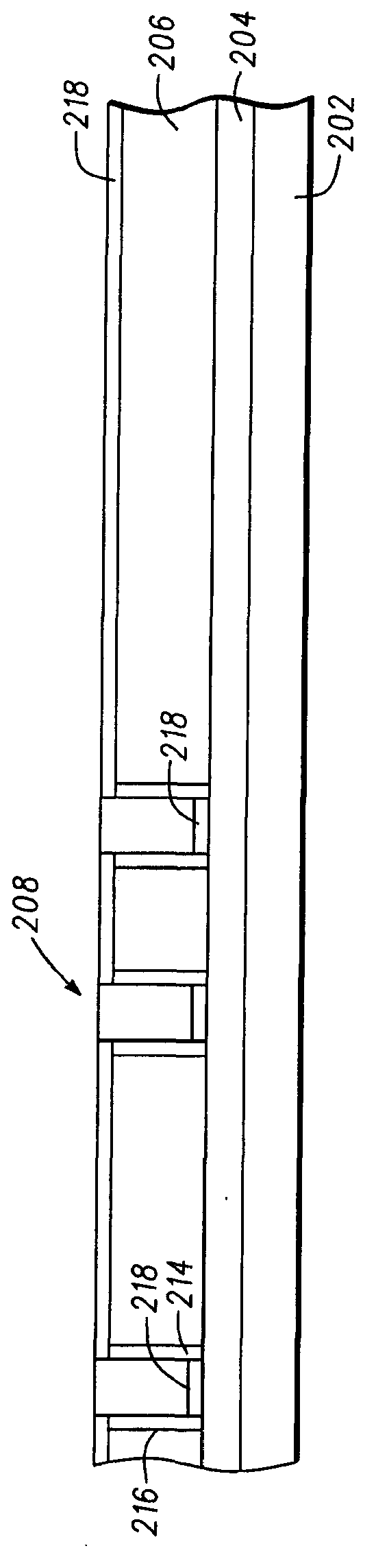
[0018] High aspect ratio vertical strips (flux guides) by integrating magnetically permeable material (typically having a magnetic permeability greater than 100, more preferably greater than 1000, such as nickel-iron alloy (NiFe)) , and the edges of the vertical bars terminate in close proximity to opposite edges and opposite sides of the magnetic sensing element, allowing part of the vertical (Z-axis) magnetic field to enter the plane of the sensing element (X-Y plane). Magnetic permeability is the degree of magnetization a material acquires in response to an applied magnetic field. These flux guides act to capture the magnetic flux from the Z component of the applied magnetic fi...


PUM


Abstract

A semiconductor process integrates three bridge circuits, each include magnetoresistive sensors coupled as a Wheatstone bridge on a single chip to sense a magnetic field in three orthogonal directions. The process includes various deposition and etch steps forming the magnetoresistive sensors and a plurality of flux guides on one of the three bridge circuits for transferring a ''Z'' axis magnetic field onto sensors orientated in the XY plane.

Description

technical field [0001] The present invention relates generally to the field of magnetoelectronic devices, and more particularly to the process of integrating CMOS compatible magnetoelectronic magnetic field sensors for sensing magnetic fields along three orthogonal directions on a single chip. Background technique [0002] Sensors are widely used in modern systems to measure or detect physical parameters such as position, motion, force, acceleration, temperature, pressure, etc. While many different sensor types exist for measuring these and other parameters, they all suffer from various limitations. For example, inexpensive low-field sensors such as those used in electronic compasses and other similar magnetic sensing applications often include anisotropic magnetoresistance (AMR) based devices. In order to obtain the required sensitivity and appropriate resistance well matched with CMOS, the size of the sensing unit of this sensor is generally on the order of square millime...

Claims


Application Information

Patent Timeline
IPC IPC(8): G01R33/02
CPCG01R33/093G01R33/0052H01L27/22B82Y25/00H01L43/12G01R33/098H10N59/00H10N50/01H10B61/00H10N50/10H10N50/80G01R33/09
Inventor R·韦格P·马瑟K·史密斯S·阿加瓦尔J·斯劳特
Owner EVERSPIN TECHNOLOGIES
Why Eureka
Try Eureka