Ultra wide wave band near-infrared electromagnetic wave absorber

A near-infrared and absorber technology, applied in instruments, optical components, optics, etc., can solve the problems of limited size and area, high production cost, and reduced production repeatability, and achieve large-area production integration, perfect absorption effect, and wide The effect of applying the foreground

Inactive Publication Date: 2013-02-13
NANJING UNIV
View PDF2 Cites 11 Cited by
  • Summary
  • Abstract
  • Description
  • Claims
  • Application Information

AI Technical Summary

Problems solved by technology

This type of absorber has complex structural design, limited size and area, and high manufacturing cost, making it difficult to effectively promote and apply this type of absorber
At present, researchers broaden the absorption bandwidth by combining resonance units with different resonance frequency bands to obtain multiple absorption frequency bands, but this further increases the difficulty of the manufacturing process and reduces the repeatability of production, which limits the practicability of this type of absorber.

Method used


Image

  • Ultra wide wave band near-infrared electromagnetic wave absorber
  • Ultra wide wave band near-infrared electromagnetic wave absorber
  • Ultra wide wave band near-infrared electromagnetic wave absorber

Examples


Embodiment 1

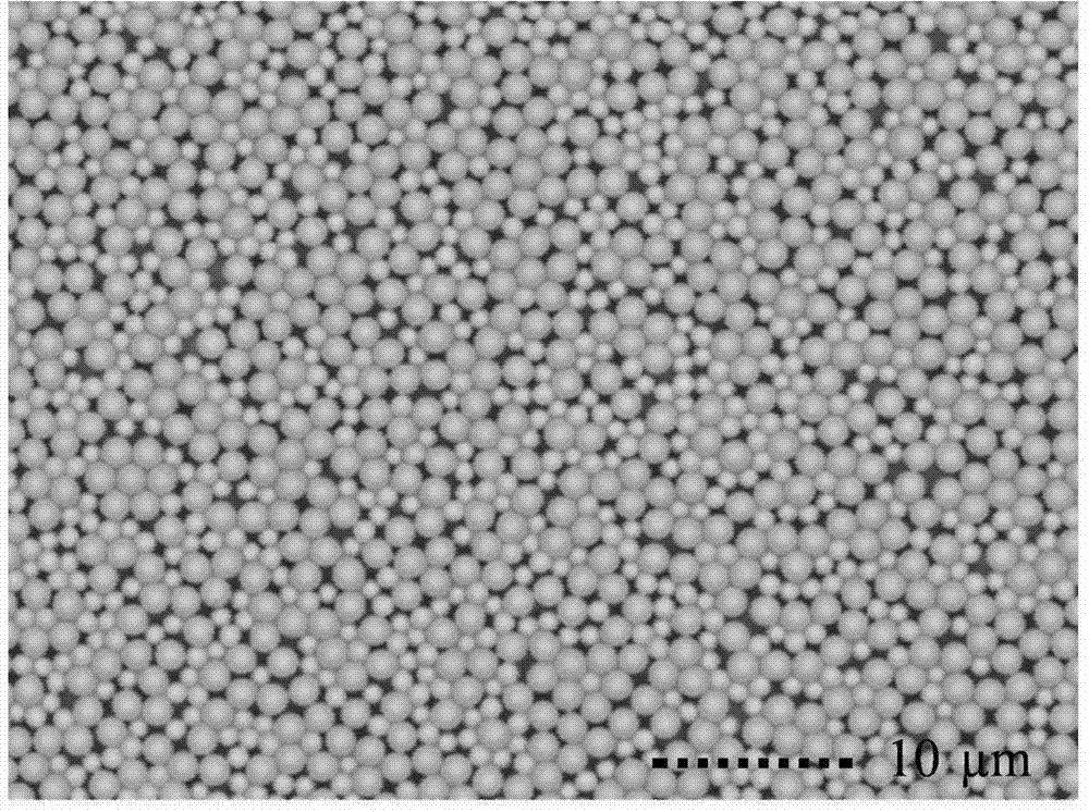
[0028] see figure 1 , the present embodiment selects two kinds of monodisperse polystyrene microspheres (i.e. dielectric spheres), the diameters of which are 1080 nanometers and 1570 nanometers, and the mixing volume ratio is 1:1; A gold film with a thickness of 100 nanometers was deposited by the method; secondly, a two-dimensional mixed dielectric ball array was self-assembled on the gold film substrate; and then the surface of the two-dimensional dielectric ball array was self-assembled by argon ion sputtering coating method Directly deposit a layer of gold film with a thickness of 13 nm;

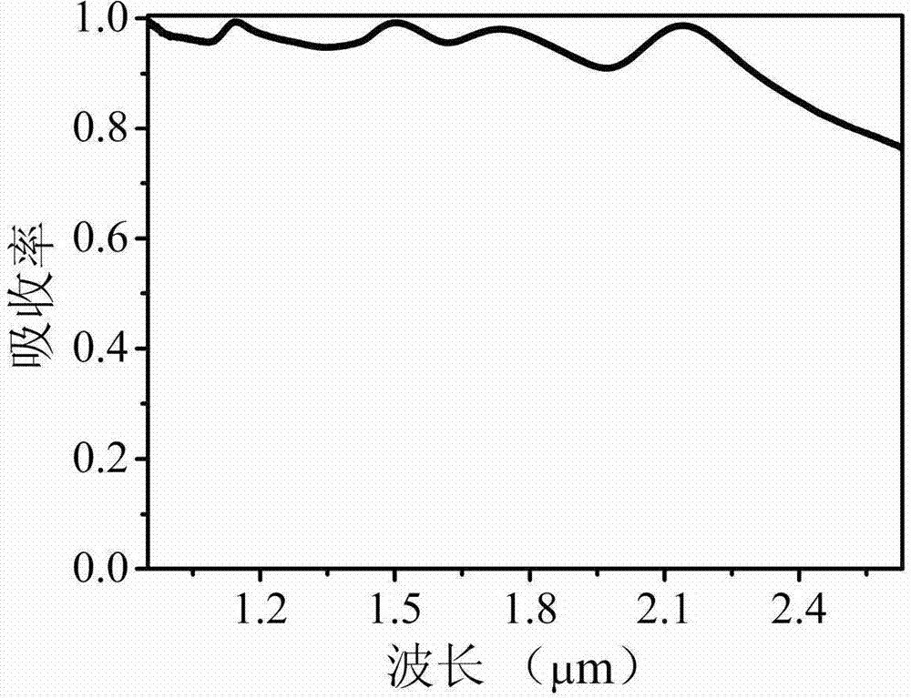
[0029] see figure 2 , the experimental results show that the ultra-broadband near-infrared absorber exhibits absorption rates of 99.7%, 98.1% and 98.7% at wavelengths of 1.497 microns, 1.735 microns and 2.139 microns respectively; In the band, the absorption rate exceeds 90%, reaching a near-perfect absorption of an ultra-wide spectrum.

Embodiment 2

[0031] In this embodiment, two kinds of monodisperse polystyrene microspheres are selected, the diameters of which are 1080 nm and 1570 nm, and the mixing volume ratio is 1:1; A gold film of 100 nanometers; secondly, self-assemble a two-dimensional mixed array of dielectric ball arrays on the gold film substrate. Then, a gold film with a thickness of 16 nanometers is directly deposited on the surface of the two-dimensional dielectric ball array by argon ion sputtering coating method;

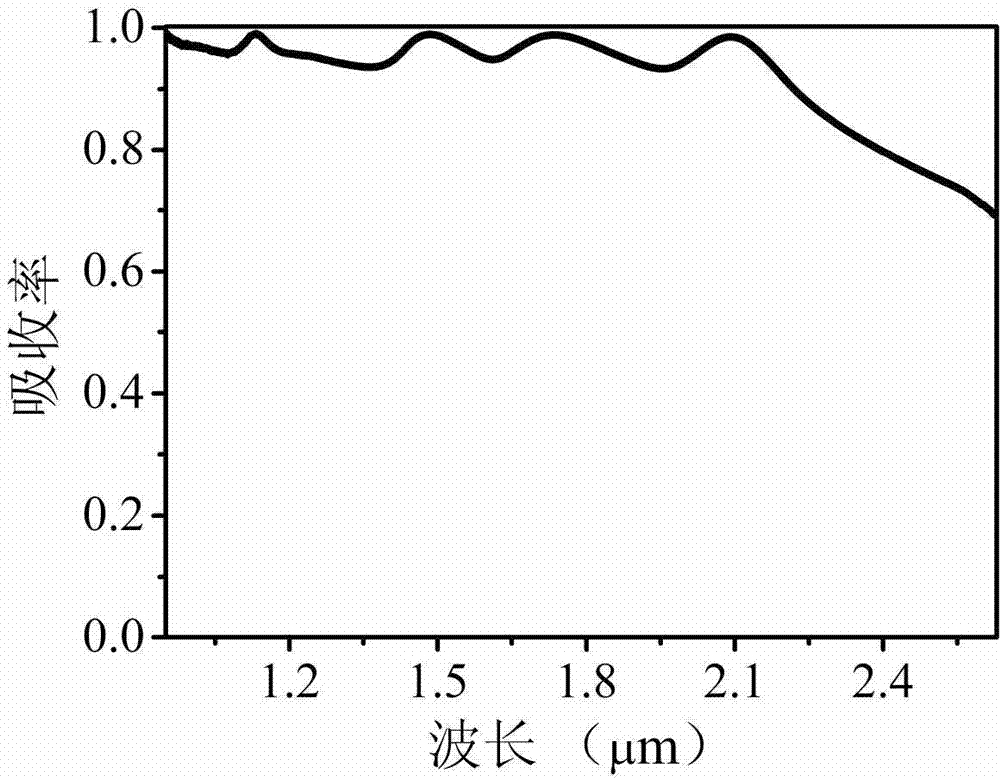
[0032] see image 3 , the experimental results show that the ultra-broadband near-infrared absorber exhibits absorption rates of 98.9%, 98.8% and 98.5% at wavelengths of 1.486 microns, 1.731 microns and 2.089 microns respectively; In the band, the absorption rate exceeds 90%, reaching a near-perfect absorption of an ultra-wide spectrum.

Embodiment 3

[0034] In this example, two kinds of monodisperse polystyrene microspheres are selected, the diameters of which are 1080 nm and 1570 nm, and the mixing volume ratio is 1:1; A gold film of 100 nanometers; secondly, self-assemble a two-dimensional mixed array of dielectric ball arrays on the gold film substrate. Then, a gold film with a thickness of 20 nanometers is directly deposited on the surface of the two-dimensional dielectric ball array by argon ion sputtering coating method;

[0035] see Figure 4 , the experimental results show that the ultra-broadband near-infrared absorber exhibits absorption rates of 97.5%, 98.8% and 98.7% at wavelengths of 1.467 microns, 1.754 microns and 2.056 microns respectively; In the band, the absorption rate exceeds 90%, reaching a near-perfect absorption of an ultra-wide spectrum.


PUM


Abstract

The invention discloses an ultra wide wave band near-infrared electromagnetic wave absorber which comprises a substrate, a first metal film, a second metal film and monolayer medium ball arrays. The first metal film is deposited on the substrate with the thickness of more than 100 nanometers and the monolayer medium ball arrays of different sizes and / or different materials are mixed and arranged on the first metal film. The second metal film is deposited on the monolayer medium ball arrays. The ultra wide wave band near-infrared electromagnetic wave absorber has a perfect absorption effect on ultra wide wave band near-infrared electromagnetic waves of large incidence and is not sensitive to polarization of the near-infrared electromagnetic waves. The ultra wide wave band near-infrared electromagnetic wave absorber has the advantages of being simple in craft, low in cost, high in repetition and capable of mass production and being possessed with wide application prospect in fields such as electromagnetic probing, absorbing and transforming.

Description

technical field [0001] The invention relates to an ultra-broadband near-infrared absorber, specifically a novel ultra-broadband near-infrared electromagnetic wave perfect absorption structure, which can be used in the fields of near-infrared electromagnetic wave absorption, detection, and thermal radiation instruments. Background technique [0002] The traditional near-infrared electromagnetic wave artificial electromagnetic material (Meta materials) perfect absorber is based on the resonance absorption of a single frequency band generated by a single-size plasmon resonance structure, and the two-band resonance generated by two or more complex plasmon resonance structures of different sizes. Resonant absorption of one or more discrete frequency bands. This type of absorber has complicated structural design, limited size and area, and high manufacturing cost, making it difficult to effectively popularize and apply this type of absorber. At present, researchers broaden the ab...

Claims


Application Information

Patent Timeline
Patent Type & Authority Applications(China)
IPC IPC(8): G02B5/00
Inventor 刘正奇王振林
Owner NANJING UNIV
Why Eureka
Try Eureka