Supercharge Your Innovation With Domain-Expert AI Agents!

Metal layer etching method and metal layer mask structure

A metal layer and etching technology, applied in the direction of electrical components, semiconductor/solid-state device manufacturing, circuits, etc., to overcome thickness limitations, improve flatness, and avoid faults

Active Publication Date: 2017-03-29
SHANGHAI HUAHONG GRACE SEMICON MFG CORP
View PDF5 Cites 0 Cited by
  • Summary
  • Abstract
  • Description
  • Claims
  • Application Information

AI Technical Summary

Problems solved by technology

[0006] The purpose of the present invention is to provide a metal interconnection etching method to solve the problems and difficulties encountered in the thick metal layer etching mentioned in the background art

Method used


Image

  • Metal layer etching method and metal layer mask structure
  • Metal layer etching method and metal layer mask structure
  • Metal layer etching method and metal layer mask structure

Examples


Embodiment Construction

[0035] The invention provides an etching method of a metal layer, so as to improve the flatness of the sidewall surface of the thick metal layer after etching, and improve the consistency of key dimensions and inductance performance after detection after development and detection after etching. Utilizing the etching method of the present invention can also overcome the limitation of the thickness of the photoresist layer.

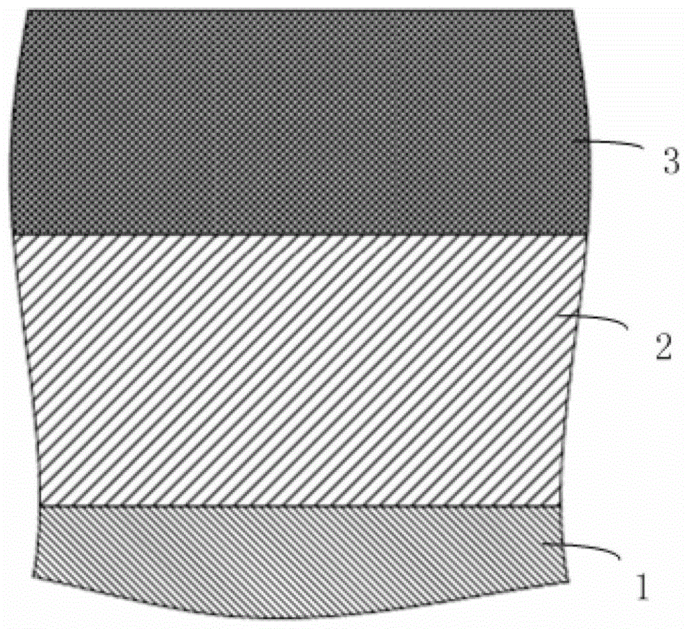
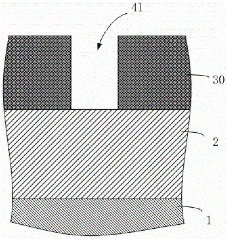
[0036] Please refer to Figure 7 , Figure 7 It is a schematic flow chart of the etching method of the embodiment of the present invention, please refer to it in each step figure 1 and Figure 8 to Figure 12 .

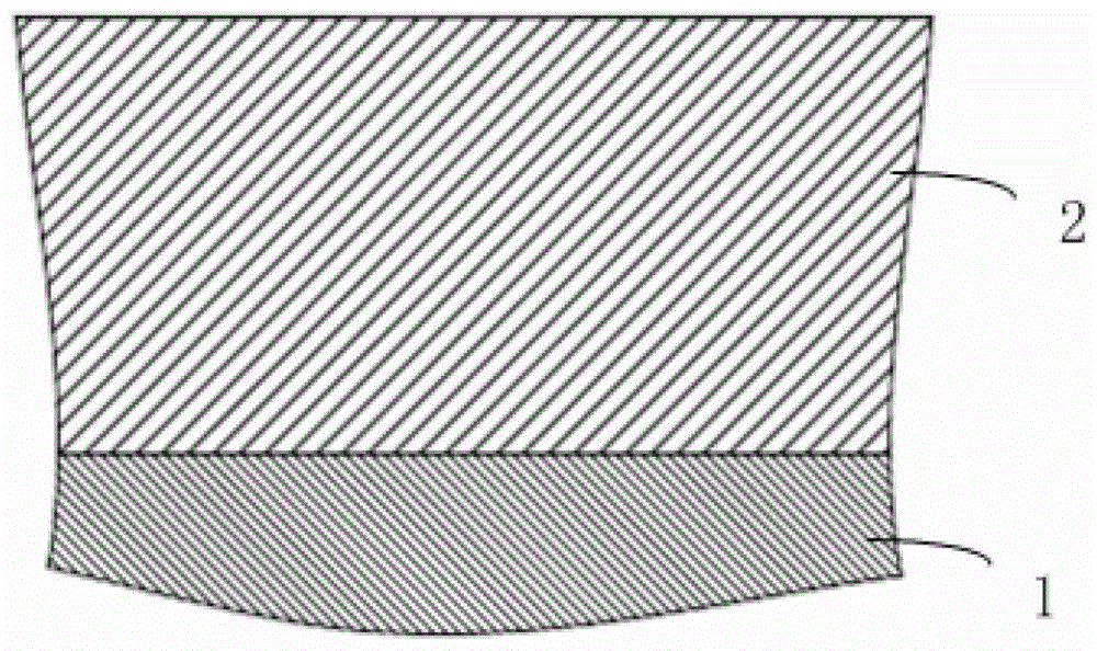
[0037] Step S1, please refer to figure 1 In the etching method of the thick metal layer 2 provided in this embodiment, firstly, a semiconductor structure is provided, and the semiconductor structure includes the metal layer 2 . The semiconductor structure may be a wafer, and the wafer may be a typical semiconductor wafer made of silicon, or a...


PUM

PropertyMeasurementUnit
thicknessaaaaaaaaaa
thicknessaaaaaaaaaa
thicknessaaaaaaaaaa

Abstract

The invention provides an etching method and a mask structure of a metal layer. The method comprises the steps as follows: providing a semiconductor structure which comprises a metal layer; forming a medium layer to cover the metal layer; forming a hard mask layer to cover the medium layer; forming a photoresist layer to cover the hard mask layer; exposing and developing the photoresist layer, patterning the photoresist layer to form a photoresist mask layer and exposing a part of the hard mask layer by the photoresist mask layer; and etching the exposed hard mask layer, the medium layer and the metal layer, and arranging the medium layer and the metal layer under the exposed hard mask layer. By adopting the etching method of the metal layer, disclosed by the invention, owing to the use of the hard mask layer and the medium layer, the photoresist layer (or the photoresist mask layer) is no longer etched in the process of etching the thick metal layer, so that overmuch polymers can not be formed on the surface of the side wall, the condition that the side wall fractures due to the overmuch polymers is avoided, and the flatness of the side wall is increased.

Description

technical field [0001] The invention relates to the field of semiconductor manufacturing, in particular to an etching method of a metal layer and a mask structure of the metal layer. Background technique [0002] In the manufacturing process of semiconductor integrated circuits, a metal layer will be formed in and / or on the semiconductor wafer or substrate, and the corresponding metal interconnection lines will be formed by etching the metallization layer, thereby forming the required semiconductor components ( Such as transistors, inductors, capacitors and resistors) and semiconductor integrated circuit structures. [0003] In the prior art in the art, photoresist is usually required to etch the metal layer. Photoresist, also known as photoresist (photo resist, PR), is a light-sensitive mixed liquid composed of three main components: photosensitive resin, sensitizer and solvent. The thickness of the photoresist layer is generally not less than 1 micron. This is because i...

Claims


Application Information

Patent Timeline
Patent Type & Authority Patents(China)
IPC IPC(8): H01L21/3213C23F4/00
Inventor 黎坡
Owner SHANGHAI HUAHONG GRACE SEMICON MFG CORP
Features
  • R&D
  • Intellectual Property
  • Life Sciences
  • Materials
  • Tech Scout
  • Unparalleled Data Quality
  • Higher Quality Content
  • 60% Fewer Hallucinations
Learn More