Fixture for plating semiconductor lead frame and plating method thereof

A lead frame and semiconductor technology, applied to the surface coating liquid device, electrolysis process, electrolysis components, etc., can solve the problems of only waste copper treatment, consumption of deplating solution, serious environmental pollution, etc., and achieve economical operation The number of personnel and artificial physical strength, the effect of improving production efficiency and smooth and precise rotation

Inactive Publication Date: 2015-07-08
SHENZHEN ALLMERIT TECH
View PDF7 Cites 1 Cited by
  • Summary
  • Abstract
  • Description
  • Claims
  • Application Information

AI Technical Summary

Problems solved by technology

Deplating not only consumes a large amount of stripping solution, but also the stripped tin is difficult to recycle, and increases the length of equipment, operation time, production cost and labor. Deplating will also increase the corrosion of hangers, steel strips and spring clips. Regular replacement, at the same time, the nitric acid system is mostly used in the deplating process, the operating environment is poor, the environmental pollution is serious, and the amount of waste water is large
[0005] 2. When tinning the semiconductor lead frame, the side ribs, middle ribs and horizontal ribs are also plated with tin coating. The cut side ribs, middle ribs and horizontal ribs waste a lot of tin, and these cut side ribs are returned It is inconvenient to recycle the , middle and horizontal bars, because the copper surface is plated with tin layer, and the mixture of copper and tin is difficult to separate, so that the cut side bars, middle bars and horizontal bars cannot be recycled and reused, and can only be treated as waste copper, and the The price of waste copper treatment is also very low, resulting in serious waste, which is a technical problem that needs to be solved for packaging factories in this industry.

Method used


Image

  • Fixture for plating semiconductor lead frame and plating method thereof
  • Fixture for plating semiconductor lead frame and plating method thereof
  • Fixture for plating semiconductor lead frame and plating method thereof

Examples


Embodiment Construction

[0041] Below in conjunction with accompanying drawing and embodiment the present invention will be further described

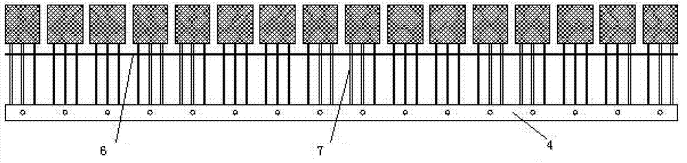
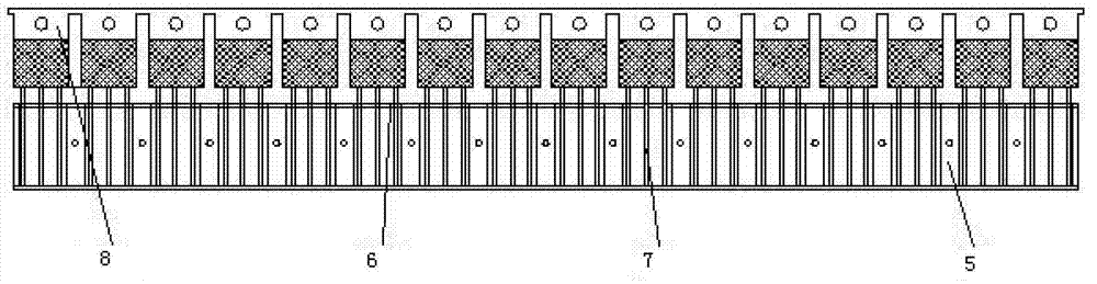
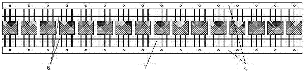
[0042] The jig for semiconductor lead frame electroplating includes a lower piece, an upper piece, and a shaft-torsion spring mechanism. The lower piece is a flat metal piece, and the jaw part of the lower piece is electrically connected to the clamped rib of the semiconductor lead frame. The upper piece is punched and bent. The shape and size of the rubber pad are the same as that of the jaw, and the front edge of the rubber pad is provided with a brush-like thin Brush, the fine brush is placed on the inner side of the clamped rib of the semiconductor lead frame, the rubber pad is silicone rubber, fluororubber or other acid-resistant rubber, the straight piece is followed by a curved surface, the curved surface is followed by a plane, and the rear end of the plane is a pressure handle , the rotating shaft-torsion spring mechanism includes a rotating shaft ins...


PUM


Abstract

The invention discloses a fixture for plating a semiconductor lead frame and a plating method thereof. Only a clamp port of a lower piece of the fixture is electrically connected with a to-be-clamped rib of the semiconductor lead frame, and other parts are electrically insulated. The plating method includes the steps that when the lead frame is a unilateral rib, only the fixture with the clamp port with the same shape with a side rib is used for fixing the side rib for plating; when the lead frame is only provided with a middle rib, only the fixture with the clamp port with the same shape with the middle rib is used for fixing the middle rib for plating; and if the lead frame is a bilateral rib, one side rib is coated with an insulation paste, and the fixture is used for clamping the other side rib for the plating. A side rib glue spreader comprises a horizontally annularly circular chain sprocket drive mechanism, a feeding bracket, a blanking retaining board, a glue spreading mechanism, an air knife, a drying groove and a hot wind cover. The fixture has the advantages that the side rib or the middle rib can be prevented from being plated by a tin coating, materials are saved, and the side rib and the middle rib can be recovered directly; and the operation is convenient, the process is reliable, production and labor costs can be reduced, production efficiency can be improved, and a deplating process of the plating fixture can be omitted.

Description

technical field [0001] The invention belongs to the technical field of electroplating, in particular relates to automatic continuous electroplating production and partial electroplating technology, in particular to an electroplating jig for a semiconductor lead frame. Background technique [0002] When the semiconductor lead frame is stamped and formed, in order to facilitate the batch and large-scale production, positioning and strength requirements of subsequent packaging processes such as Die Bonding, Wire Bonding, Modeling and Plating, special Side ribs, middle ribs and transverse ribs are designed, and individual forms also adopt the form of double-sided ribs or peripheral ribs, and most of them are single-sided ribs. With the miniaturization and miniaturization of devices, there are more and more forms of double-sided ribs and quadrilateral ribs. Side ribs, middle ribs and transverse ribs are all technical ribs, which need to be cut off after the electroplating proces...

Claims


Application Information

Patent Timeline
Patent Type & Authority Patents(China)
IPC IPC(8): C25D17/08C25D5/02B05C1/06B05C13/02
Inventor 毕翊李海燕
Owner SHENZHEN ALLMERIT TECH
Why Eureka
Try Eureka