Unlock instant, AI-driven research and patent intelligence for your innovation.

Alignment mark and manufacturing method thereof

An alignment mark and manufacturing method technology, applied in semiconductor/solid-state device manufacturing, electrical components, electrical solid-state devices, etc., can solve problems such as inability to align, decrease alignment accuracy, and difficulty in obtaining alignment marks, and achieve easy access. Effect

Active Publication Date: 2013-02-27
SHANGHAI HUAHONG GRACE SEMICON MFG CORP
View PDF5 Cites 22 Cited by
  • Summary
  • Abstract
  • Description
  • Claims
  • Application Information

AI Technical Summary

Problems solved by technology

[0010] The purpose of the present invention is to provide an alignment mark and its manufacturing method, so as to solve the problems of difficulty in obtaining alignment marks, decreased alignment accuracy or failure to align

Method used


Image

  • Alignment mark and manufacturing method thereof
  • Alignment mark and manufacturing method thereof
  • Alignment mark and manufacturing method thereof

Examples


Embodiment Construction

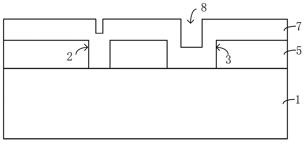
[0050] Such as Figure 4 As shown, in the prior art, the pit 91 formed on the surface of the second metal layer 9 at the position corresponding to the trench 3 is used as an alignment mark for the lithography process of the first layer metal interconnection structure. However, due to the depth of the trench 3 and the The depths of the contact holes 2 are equal and small, so the depth of the pit 91 is small, which will make it difficult to obtain the alignment marks on the silicon wafer in the subsequent lithography process, resulting in the problem of decreased alignment accuracy or inability to align .

[0051] In order to solve the above problems, the present invention forms a trench at a position corresponding to the isolation structure in the interlayer dielectric layer while forming a contact hole in the interlayer dielectric layer, and the depth of the trench extends into the isolation structure, that is, the depth of the trench The depth is greater than the depth of the...


PUM


Abstract

The invention provides an alignment mark and a manufacturing method thereof. Contact holes are formed in interlayer dielectric layers, simultaneously, grooves are formed at positions in the interlayer dielectric layers, the positions correspond to isolation structures, the grooves extend into the isolation structures, so that depth of the grooves is increased, the depth of concave pits subsequently formed on surfaces of metal layers is larger, the alignment mark on a silicon wafer can be easily obtained in subsequent lithography processes, and problems that alignment accuracy is decreased or alignment can't be performed can not be caused.

Description

technical field [0001] The invention relates to an alignment mark and a manufacturing method thereof, in particular to an alignment mark used in a lithography process of a first-layer metal interconnection structure and a manufacturing method thereof. Background technique [0002] In the manufacturing process of semiconductor components, as the components become smaller and smaller, the mask pattern is also smaller. Therefore, in the photolithography process, in order to transfer the mask pattern to the silicon wafer accurately, it is usually necessary Several alignment marks are formed on the chip for alignment of the mask (mark), so that the mask pattern can be accurately copied to the desired position on the silicon wafer. [0003] During the manufacturing process of semiconductor elements, steps and grooves are often formed on the surface of the silicon wafer. The steps and grooves are like marks on the silicon wafer, and such marks can be used as alignment marks in the ...

Claims


Application Information

Patent Timeline
IPC IPC(8): H01L23/544H01L21/762
Inventor 黎坡林伟铭张瑛李佳佳莘海维钟政纪登峰奚裴
Owner SHANGHAI HUAHONG GRACE SEMICON MFG CORP
Features
  • R&D
  • Intellectual Property
  • Life Sciences
  • Materials
  • Tech Scout
  • Unparalleled Data Quality
  • Higher Quality Content
  • 60% Fewer Hallucinations
Learn More