Silicon on insulator structure and semiconductor device structure

A silicon-on-insulator, device structure technology, applied in semiconductor devices, electrical solid devices, electrical components, etc., can solve the problems of parasitic capacitance that cannot meet product requirements, and parasitic capacitance becomes larger.

Inactive Publication Date: 2013-02-27
SHANGHAI HUAHONG GRACE SEMICON MFG CORP
View PDF8 Cites 11 Cited by
  • Summary
  • Abstract
  • Description
  • Claims
  • Application Information

AI Technical Summary

Problems solved by technology

The thickness of the buried oxide layer 102 is preferably equivalent to the thickness of the positive gate oxide layer, generally However, in the above-mentioned semiconductor devices formed on silicon-on-insulator, the parasitic capacitance between the device and the silicon base layer will increase due to the reduction of the thickness of the buried oxide layer. In some high-frequency applications, the parasitic capacitance changes Big is unable to meet product requirements

Method used


Image

  • Silicon on insulator structure and semiconductor device structure
  • Silicon on insulator structure and semiconductor device structure
  • Silicon on insulator structure and semiconductor device structure

Examples


Embodiment Construction
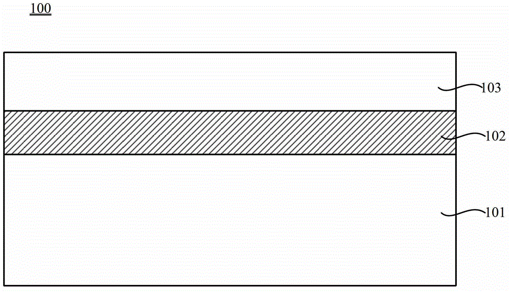
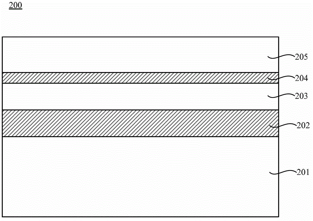
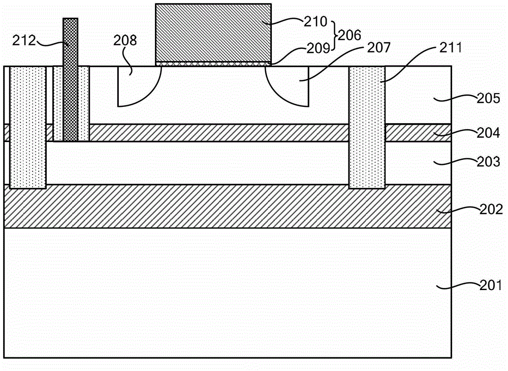
[0026] The core idea of ​​the present invention is that two layers of buried oxide layers are included in the silicon-on-insulator structure, wherein the first buried oxide layer is used to isolate the electrical connection between the first silicon layer and the third silicon layer. connection; while the second buried oxide layer is used for some kind of insulating layer of the semiconductor device, so it is the second buried oxide layer that mainly affects the parasitic capacitance of the semiconductor device. In the above silicon-on-insulator structure, a better isolation effect can be achieved by thickening the thickness of the first buried oxide layer, and at the same time, by reducing the thickness of the second buried oxide layer, the isolation effect can be Next, the purpose of reducing the parasitic capacitance of the semiconductor device on the silicon-on-insulator structure is achieved.

[0027] In order to make the content of the present invention clearer and easie...


PUM


Abstract

The invention provides a silicon on insulator structure and a semiconductor device structure. The silicon on insulator structure comprises a first silicon layer, a first buried oxide layer formed on the first silicon layer, a second silicon layer formed on the first buried oxide layer, a second buried oxide layer formed on the second silicon layer, and a third silicon layer formed on the second buried oxide layer. By adopting the silicon on insulator structure, a double gate transistor structure can be utilized, and the stray capacitance between the semiconductor device which is arranged on the silicon on insulator structure and a substrate is effectively reduced.

Description

technical field [0001] The invention relates to the field of semiconductor manufacturing, more specifically, the invention relates to a silicon-on-insulator structure and a semiconductor device structure using the silicon-on-insulator structure. Background technique [0002] Silicon-on-insulator (SOI, Silicon-on-insulator) is being used more and more widely as the demand for faster speed and lower temperature of semiconductor devices emerges. The main feature of the silicon-on-insulator structure is that an insulating layer (buried oxide layer) is inserted between the active layer and the substrate layer to isolate the electrical connection between the active layer and the substrate. The device brings many advantages such as small parasitic effect, fast speed, low power consumption, high integration, and strong radiation resistance. [0003] Double gate (double gate) transistors have better scaling characteristics than conventional single gate transistors. Generally, the s...

Claims


Application Information

Patent Timeline
Patent Type & Authority Applications(China)
IPC IPC(8): H01L27/12H01L29/78
Inventor 李乐
Owner SHANGHAI HUAHONG GRACE SEMICON MFG CORP
Why Eureka
Try Eureka