

Pixel driving structure, driving method and display device
A technology for driving structures and pixels, applied in static indicators, nonlinear optics, instruments, etc., can solve the problems of high power consumption and high cost of pixel driving structures, and achieve the effects of reducing power consumption, reducing voltage swing, and reducing costs
- Summary
- Abstract
- Description
- Claims
- Application Information
AI Technical Summary
Problems solved by technology
Method used
Image

Examples
Embodiment 1
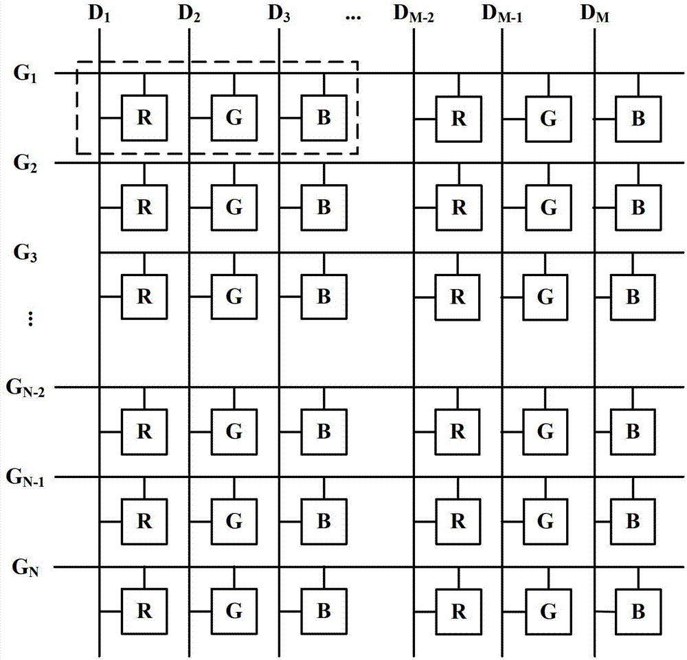
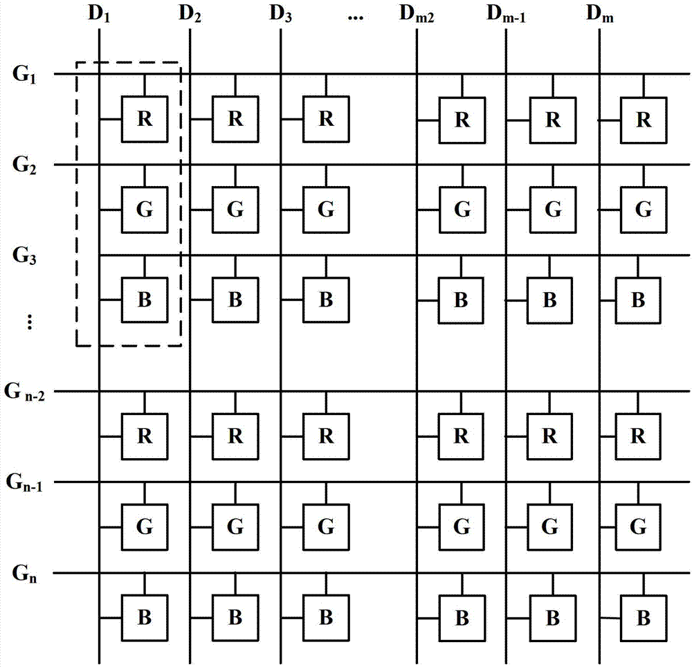
[0033] Embodiment 1 of the present invention provides a pixel driving structure, for details, please refer to Figure 5 , Image 6 The schematic structural diagram of the pixel driving structure shown, the pixel driving structure includes M data lines and N scanning lines, and the M data lines are vertically arranged in columns and parallel to each other (such as Figure 5~Figure 6 D shown 1 、D 2 、D 3 ,...,D M-1 、D M ), the N scanning lines are arranged horizontally and parallel to each other (such as Figure 5~Figure 6 G shown 1 , G 2 , G 3 , G 4 , G 5 , G 6 ,...,G N-1 , G N ), the M and N are positive integers, where:
[0034] The M data lines intersect with the N scan lines to form a plurality of pixel units arranged in a matrix, wherein each pixel unit includes at least any two sub-pixels among the four sub-pixels of R, G, B, and W , for example: each pixel unit may include two sub-pixels R and G, or two sub-pixels R and B, or two sub-pixels R and W, or two ...
Embodiment 2
[0063] Embodiment 2 of the present invention provides a display device, which includes the pixel driving structure described in Embodiment 1.
[0064] Specifically, the display device can be any product or component with a display function such as a liquid crystal panel, an electronic paper, an OLED panel, a mobile phone, a tablet computer, a television set, a monitor, a notebook computer, a monitor, a notebook computer, a digital photo frame, a navigator, etc. .
Embodiment 3
[0066] Embodiment 3 of the present invention provides a driving method of the pixel driving structure described in Embodiment 1, the method comprising:
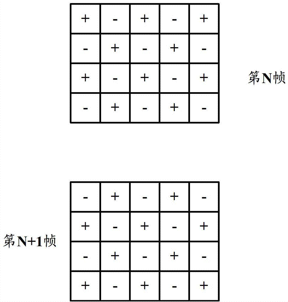
[0067] When displaying a frame of pixel images, a signal greater than the reference voltage (voltage deflection polarity is "+") is input to one of any two adjacent data lines among the M data lines, and the other The data line inputs a signal lower than the reference voltage (voltage deflection polarity is "-"), and the M is a positive integer.
[0068] It should be noted that, for the same data line, when displaying any two adjacent frames of pixel images, the input voltage on the data line will be greater than the reference voltage (the voltage deflection polarity is "+") and less than The reference voltage (the polarity of the voltage deflection is "-") is changed, and it is not fixed.
[0069] When the driving method described in the second embodiment of the present invention is used to drive the pixel driving structure...
PUM
 Abstract
Description
Claims
Application Information