Display, method of manufacturing the same and electric apparatus
A technology of electronic equipment and display, applied in semiconductor/solid-state device manufacturing, circuits, electrical components, etc., can solve problems such as changing TFT characteristics, threshold level voltage shift, etc., and achieve the effect of suppressing degradation
Active Publication Date: 2013-03-06
JOLED INC
View PDF10 Cites 8 Cited by
- Summary
- Abstract
- Description
- Claims
- Application Information
AI Technical Summary
Problems solved by technology
However, if light (especially ultraviolet light of 420nm or less) is irradiated on a semiconductor layer made of an oxide semiconductor, its TFT characteristics, or more specifically, its threshold level voltage ( Vth) may be shifted to the negative (-) direction
Method used
View moreImage
Smart ImageViewing Examples

Examples
Embodiment approach
[0034] 1-1. Overall structure
[0035] 1-2. The overall structure of the display
[0036] 1-3. Manufacturing method
Login to View More PUM
 Abstract
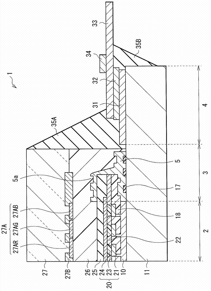
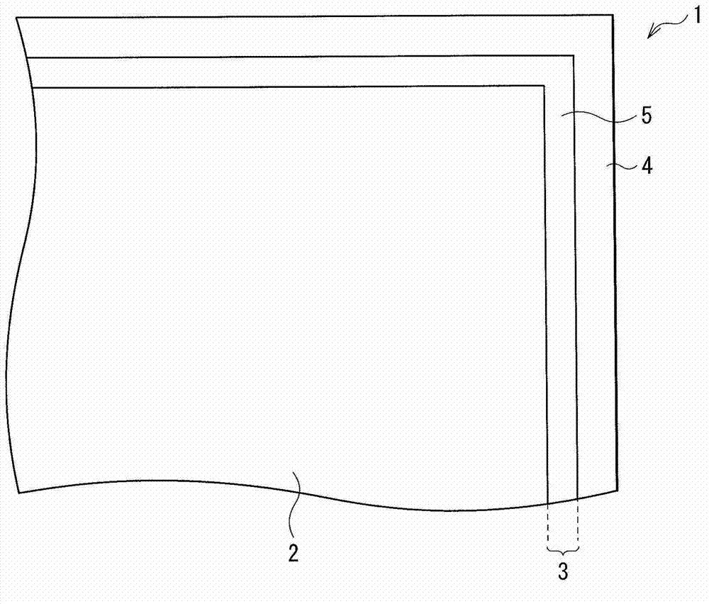
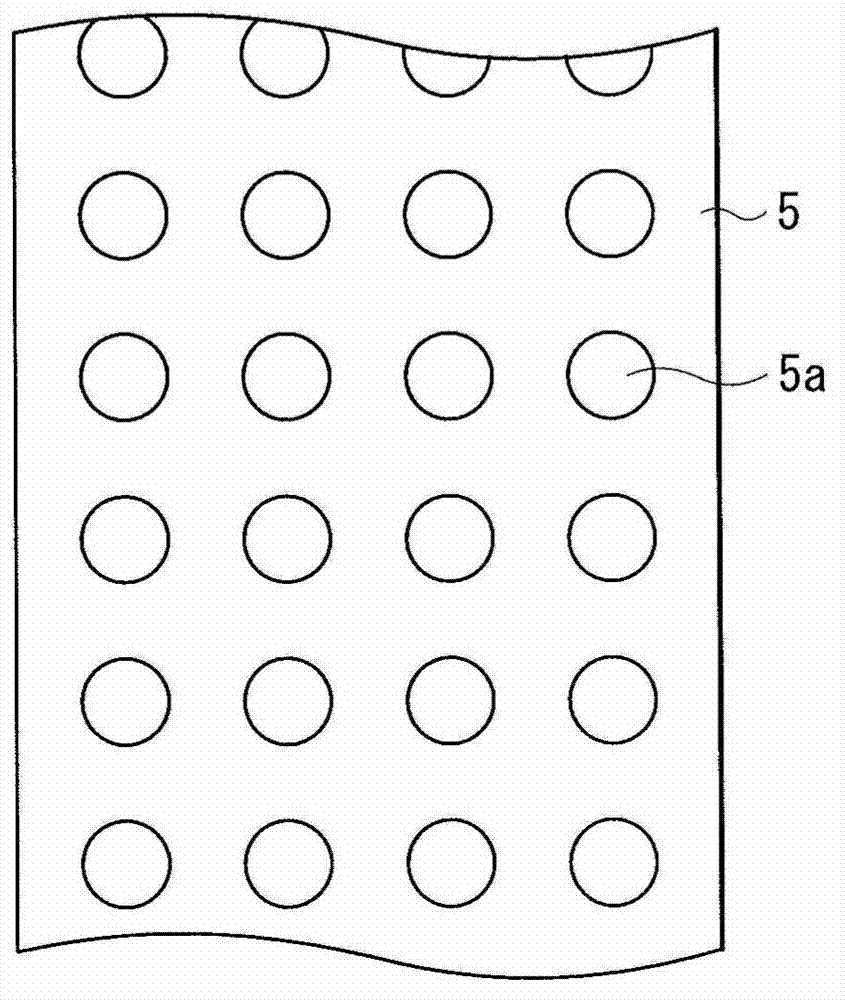
A display, a method of manufacturing the display, and an electronic apparatus are provided. The display includes a resin, a transistor; and a light shielding material positioned between the resin and the transistor. The light shielding material is configured to suppress an incidence of light on the transistor. Light is prevented from entering an oxide semiconductor layer to be used as an active layer so as to suppress deterioration of transistor characteristics.
Description
Technical field [0001] The present disclosure relates to a display using a thin film transistor (TFT) whose active layer is made of an oxide semiconductor and a method of manufacturing the display. Background technique [0002] As a basic technology, TFT is widely used in liquid crystal displays, organic EL displays, etc. Generally, the semiconductor layer used as the active layer of the TFT is made of amorphous silicon (a-Si:H) or polysilicon, but in recent years, oxides such as metal oxides formed by inexpensive equipment such as magnetron sputtering have been used. Semiconductors are also used to form such semiconductor layers. However, if light (especially ultraviolet light of 420 nm or shorter) is irradiated on a semiconductor layer made of an oxide semiconductor, it may change its TFT characteristics due to light induction, or more specifically, its threshold level voltage ( Vth) may shift to the negative (-) direction. [0003] To solve this problem, for example, Japanese...
Claims
Login to View More Application Information
Patent Timeline
 Patent Type & Authority Applications(China)
IPC IPC(8): H01L29/786H01L23/552H01L27/32H01L21/77
CPCH01L2924/0002H01L27/3272H01L27/1225H01L23/552H10K59/126H01L2924/00
Inventor 中平忠克
Owner JOLED INC
Features
- R&D
- Intellectual Property
- Life Sciences
- Materials
- Tech Scout
- Unparalleled Data Quality
- Higher Quality Content
- 60% Fewer Hallucinations
Learn More Browse by: Latest US Patents, China's latest patents, Technical Efficacy Thesaurus, Application Domain, Technology Topic, Popular Technical Reports.
© 2025 PatSnap. All rights reserved.Legal|Privacy policy|Modern Slavery Act Transparency Statement|Sitemap|About US| Contact US: help@patsnap.com