Digital time delay lock loop circuit

A technology of digital delay and locked loop, which is applied in the direction of electrical components, automatic power control, etc., can solve the problems of long cycle number, delay locked loop error locking, etc.

Active Publication Date: 2013-03-06
EHIWAY MICROELECTRONIC SCI & TECH SUZHOU CO LTD
View PDF7 Cites 48 Cited by
  • Summary
  • Abstract
  • Description
  • Claims
  • Application Information

AI Technical Summary

Problems solved by technology

[0005] Since the traditional delay-locked loop uses counters and frequency dividers to adjust the delay amount of the digital control delay chain, it takes a long number of cycles to comp...

Method used


Image

  • Digital time delay lock loop circuit
  • Digital time delay lock loop circuit
  • Digital time delay lock loop circuit

Examples


Embodiment Construction

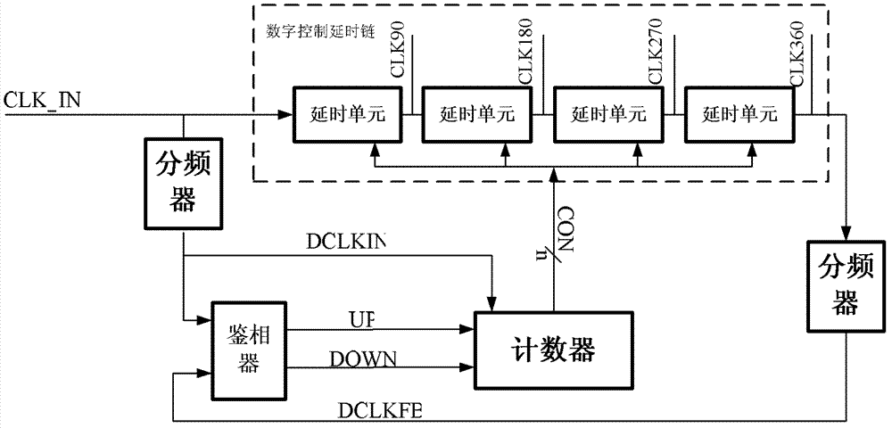
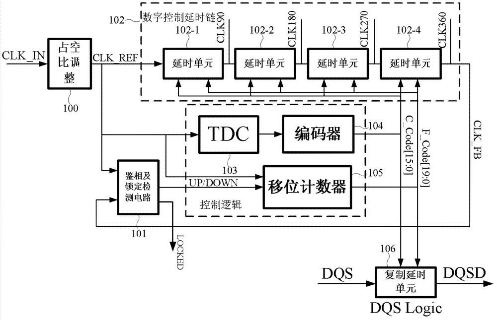
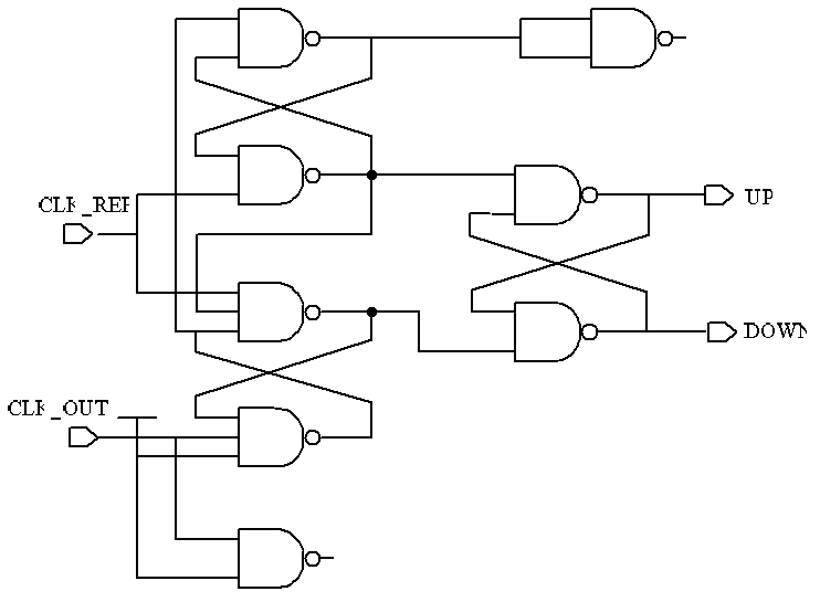
[0040] see figure 2 , 5 , 8, a kind of fast locking digital time-delay locked loop circuit of the present invention, comprises duty cycle adjustment circuit 100, phase discrimination and lock detection circuit 101, digital control delay chain 102, digital time converter 103, shift counter 105 and copy delay unit 106. The duty cycle adjustment circuit is connected to the input clock and the reference clock; the reference clock is input to one end of the phase detector, the input end of the digital control delay chain and the input end of the time-to-digital converter; the output of the digital control delay chain is connected to the phase detector The other input end of device; The output of phase detector connects the input end of shift counter; The control word that the time-to-digital converter output produces after encoder 104 receives the coarse adjustment delay unit 108 in the digital control delay chain Control word input end; the output control word of the shift coun...


PUM


Abstract

The invention discloses a quick locking type digital time delay lock loop circuit and relates to the technology of signal phase deviation. The digital time delay lock loop circuit comprises a duty ratio adjusting circuit, a phase discriminator, a digital control time delay chain, a digital time converter, a shift counter and a replication time delay unit, wherein the digital control time delay chain comprises at least four levels of identical time delay units, all time delay units are controlled by the same controller and has the same time delay quantity; and each level of time delay units comprises a coarse tuning time delay unit and a fine tuning time delay unit, and the coarse tuning time delay unit and the fine tuning time delay unit are connected in series to expand the working frequency range of the delay lock loop. The digital time delay lock loop circuit provides an accurate 90-degree phase shift signal to a DQS (Data Strobe Signal) signal in a DDR (Data Direction Register) controller and has the properties of quickly locking and avoiding wrong lock of the loop.

Description

technical field [0001] The invention relates to the technical field of signal phase offset, and relates to a fast locking digital delay locked loop circuit for a DQS signal of a DDR controller in a field programmable gate array. Background technique [0002] Field Programmable Gate Array (FPGA) is a large-scale programmable device, which consists of programmable logic blocks (CLBs), wiring resources, and input and output blocks (IOBs). Among them, the input and output module provides dedicated data selection pulse signal (DQS) and data signal (DQ) for the DDR controller. In the DDR SDRAM controller of the FPGA, the DQS signal and the DQ data signal are generated by the DDR SDRAM memory chip and are transmitted along with the source synchronous method. It is necessary to use a delay locked loop to shift the phase of the DQS signal by 90 degrees to make it rise and The falling edge falls on the center of DQ to ensure the correct sampling. [0003] figure 1 Represents a typi...

Claims


Application Information

Patent Timeline
IPC IPC(8): H03L7/089
Inventor 杨海钢陈柱佳
Owner EHIWAY MICROELECTRONIC SCI & TECH SUZHOU CO LTD
Why Eureka
Try Eureka