Method for forming conductive plug on surface of magnetic tunnel junction (MTJ)

A magnetic tunnel junction and conductive plug technology, which is applied in the manufacture/processing of electromagnetic devices, etc., can solve the problems of breakdown or short circuit, the distance between conductive layers is reduced, and the through hole is easily over-etched, so as to avoid breakdown or short circuit. short circuit effect

Inactive Publication Date: 2013-03-13
SEMICON MFG INT (SHANGHAI) CORP
View PDF5 Cites 6 Cited by
  • Summary
  • Abstract
  • Description
  • Claims
  • Application Information

AI Technical Summary

Problems solved by technology

[0004] Usually, the magnetic tunnel junction is electrically connected to the word line and the bit line through a conductive plug, but the size of the through hole forming the conductive plug is limited by the minimum size of the photolithography and etching process, and the magnetic tunnel junction The size can be made very small, the size of the through hole is larger than the size of the magnetic tunnel junction, s

Method used


Image

  • Method for forming conductive plug on surface of magnetic tunnel junction (MTJ)
  • Method for forming conductive plug on surface of magnetic tunnel junction (MTJ)
  • Method for forming conductive plug on surface of magnetic tunnel junction (MTJ)

Examples


Embodiment Construction

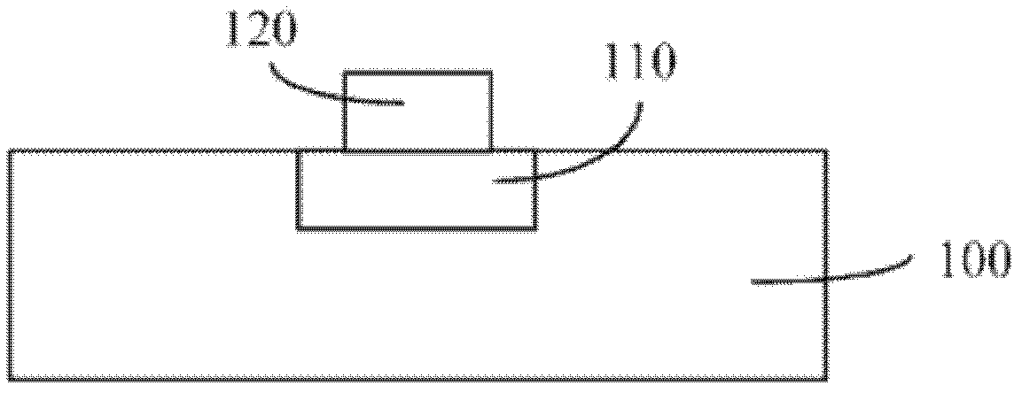
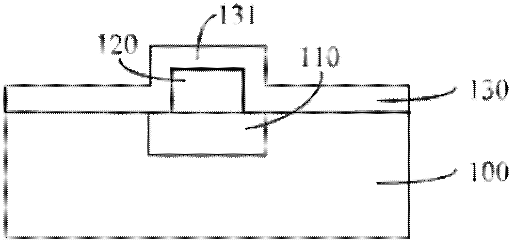
[0026] Since the size of the through hole forming the conductive plug is larger than the size of the magnetic tunnel junction, it is easy to over-etch when etching the through hole, and the dielectric layer around the magnetic tunnel junction is also etched away, resulting in The distance between the finally formed conductive plug and the conductive material below the magnetic tunnel junction becomes smaller, which may easily cause breakdown or short circuit, and seriously cause the device to be scrapped. Wherein, the size mentioned in the embodiments of the present invention refers to the lateral size of the semiconductor structure, that is, the size of the semiconductor structure in a top view of the semiconductor structure.

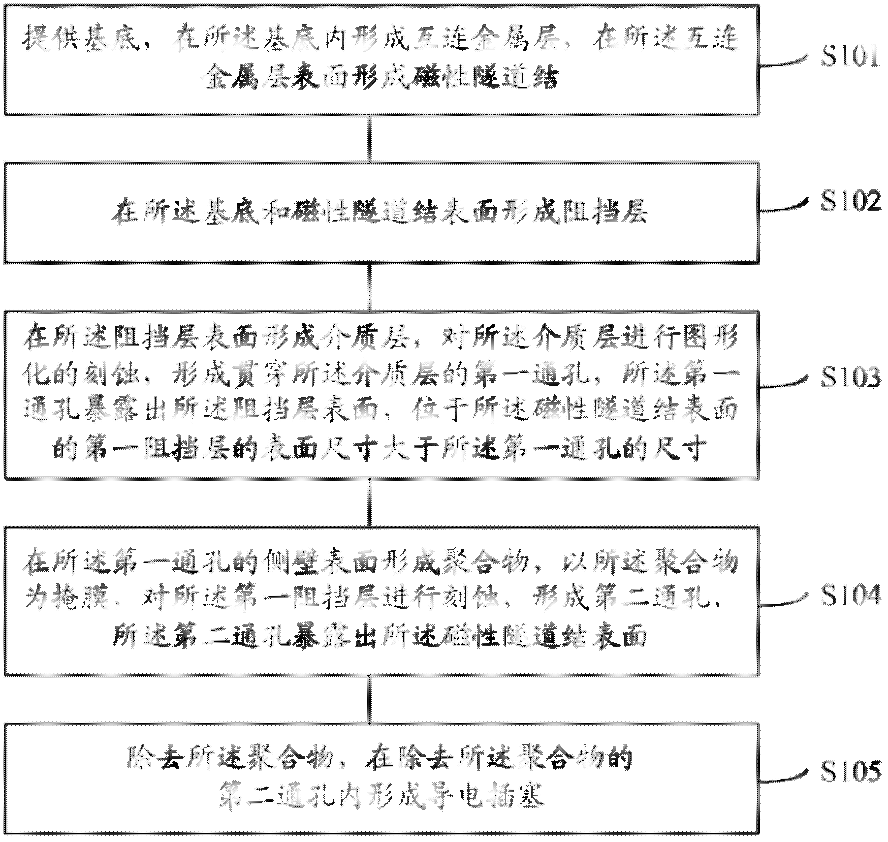
[0027] The inventor proposed a method of forming a conductive plug on the surface of the magnetic tunnel junction after research. For the schematic flow diagram of the method, please refer to figure 1 , including:

[0028] S101, providing a substrate,...


PUM


Abstract

A method for forming a conductive plug on the surface of an MTJ includes providing a substrate, forming interconnected metal layers at the bottom of the substrate, and forming the MTJ on the surface of the interconnected metal layers; forming a barrier layer on the surfaces of the substrate and the MTJ; forming a medium layer on the surface of the barrier layer, and performing imaging etching on the medium layer to form a first through hole penetrating through the medium layer, wherein the surface size of a first barrier layer on the surface of the MTJ is larger than the size of the first through hole; forming a polymer on the side wall surface of the first through hole, taking the polymer as a mask to perform etching to form a second through hole; and removing the polymer, and forming the conductive plug in the second through hole which the polymer is removed from. Short circuit or breakdown between the conductive plug and conducting materials under the MTJ can be avoided due to the fact that the surface size of the first barrier layer on the surface of the MTJ is larger than the size of the later-formed first through hole.

Description

technical field [0001] The invention relates to semiconductor manufacturing technology, and more specifically, the invention relates to a method for forming a conductive plug on the surface of a magnetic tunnel junction. Background technique [0002] Magnetic Random Access Memory (Magnetic Random Access Memory, MRAM) is a kind of solid memory, including a plurality of magnetic tunnel junctions (MTJ) or magnetic tunnel junction (MTJ) arrays as information recording carriers, and the two ends of the magnetic tunnel junction are formed There are wordlines and bitlines for the current drive lines, usually in adjacent two interconnect metal layers. The magnetic tunnel junction includes a pinned magnetic layer, a free magnetic layer, and a tunnel barrier layer between the pinned magnetic layer and the free magnetic layer, and the pinned magnetic layer has a fixed magnetic direction. When current flows through the word line and the bit line, a current magnetic field is generated, ...

Claims


Application Information

Patent Timeline
IPC IPC(8): H01L43/12
Inventor 曾贤成
Owner SEMICON MFG INT (SHANGHAI) CORP
Why Eureka
Try Eureka