Zero dead area grid driving circuit

A gate drive circuit, zero dead zone technology, applied in electrical components, electronic switches, pulse technology, etc., can solve problems such as large electromagnetic interference, increased power consumption, diode voltage jumps, etc., to reduce electromagnetic interference and prevent loss. and electromagnetic interference, the effect of improving system efficiency

Inactive Publication Date: 2013-03-13
UNIV OF ELECTRONICS SCI & TECH OF CHINA
View PDF4 Cites 18 Cited by
  • Summary
  • Abstract
  • Description
  • Claims
  • Application Information

AI Technical Summary

Problems solved by technology

[0005] However, the existence of the dead time will make the circuit work, there is a time when the switch tube PMOS and the synchronous rectifier tube NMOS are turned off at the same time
Due to the fact that the current of the inductor L cannot be mutated, the parasitic body diode of the synchronous rectifier will be turned on, resulting in a voltage jump of the conduction voltage drop of the diode, and the diode has a reverse recovery current, which will lead to an increase in power consumption
In addition, there is a large voltage change rate (dv / dt) and current change rate (di / dt) when the diode is turned on and off, which will generate large electromagnetic interference

Method used


Image

  • Zero dead area grid driving circuit
  • Zero dead area grid driving circuit
  • Zero dead area grid driving circuit

Examples


Embodiment 1

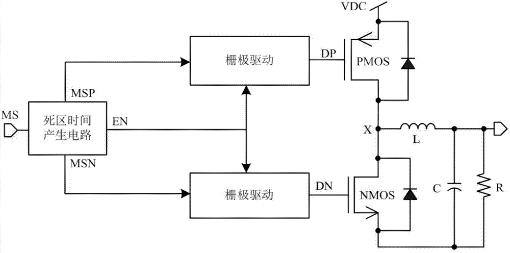
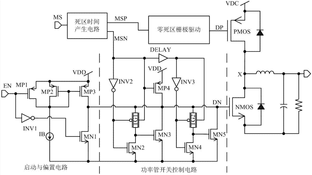
[0021] see figure 2 , is the zero-dead zone gate drive circuit of the present invention, and is used in a typical structure of a step-down voltage stabilizing circuit. The PMOS power transistor gate drive circuit and the NMOS power transistor gate drive circuit in the step-down voltage stabilizing circuit have similar structures, and both are composed of the zero dead zone gate drive circuit of the present invention. The PMOS power transistor gate drive circuit is connected between the dead time generation circuit and the PMOS power transistor, and the MOS power transistor gate drive circuit is connected between the dead time generation circuit and the NMOS power transistor gate, figure 2 Only shows the structure of NMOS power tube gate drive circuit. figure 2 In the circuit shown, except for the inductor L, the capacitor C and the load R, other components are integrated in the same chip to form a step-down regulator circuit of this example.

[0022] The gate drive circui...

Embodiment 2

[0029] In this example, the zero-dead zone gate drive circuit is used in a push-pull output circuit using PMOS power transistors and NMOS power transistors, such as various push-pull power amplifier circuits composed of field effect transistors, which constitute the gates of PMOS power transistors and NMOS power transistors. Drive circuit. The circuit of this example can also use integrated circuit technology to integrate the zero-dead zone gate drive circuit and the push-pull output circuit into the same chip to form a monolithic power amplifier.


PUM


Abstract

The invention relates to a grid driving circuit which aims at solving the starting problem of a parasitic diode generated by a grid driving circuit in the prior art. The zero dead area grid driving circuit comprises a starting and current offset circuit and a power tube switch control circuit, wherein the starting and current offset circuit comprises three P-channel metal oxide semiconductor (PMOS) tubes (an MP1, an MP2 and an MP3), an N-channel metal oxide semiconductor (NMOS) tube MN1 and an inverter INV1; and the power tube switch control circuit comprises a PMOS tube (an MP4), four NMOS tubes (an MN2, an MN3, an MN4 and an MN5), two inverters (an INV2 and an INV3), two transmission gates (a TG1 and TG2) and a delay unit (DELAY). The grid driving circuit avoids starting of the parasitic diode and avoids loss and electromagnetic interface caused by the parasitic diode. The grid driving circuit is mainly used in direct current / direct current (DC / DC) converters and various push-pull output circuits adopting PMOS power tubes and NMOS power tubes.

Description

technical field [0001] The present invention relates to a metal oxide field effect transistor or field effect transistor for short (MOSFET or MOS for short), and a drive control circuit, in particular to a gate drive for a step-down regulator circuit using a PMOS power transistor and an NMOS power transistor. circuit. Background technique [0002] MOSFET is an important component that constitutes various functional circuits, and is the most important active component in integrated circuits. Especially as a DC / DC converter for high-power applications, such as BUCK voltage regulator circuit (step-down voltage regulator circuit), etc., and the core component of the push-pull output circuit, it has a very wide range of uses. In the above applications, MOSFETs are generally classified into PMOS power transistors and NMOS power transistors according to their conductivity types, and their gate drive circuits generally have a similar structure. The PMOS power tube connected to the...

Claims


Application Information

Patent Timeline
Patent Type & Authority Applications(China)
IPC IPC(8): H03K17/687
Inventor 周泽坤张其营张庆玲张竹贤崔佳男吴传奎李强石跃明鑫王卓张波
Owner UNIV OF ELECTRONICS SCI & TECH OF CHINA
Why Eureka
Try Eureka