This helps you quickly interpret patents by identifying the three key elements:
Problems solved by technology
Method used
Benefits of technology
Problems solved by technology
However, a topological insulator capable of quantizing the anomalous Hall effect has not actually been fabricated
Even a ferromagnetic material (including magnetically doped topological insulator )
Method used
Image
Click on the blue label to locate the original text in one second.
Reading with bidirectional positioning of images and text.
Examples
Embodiment 1
[0069] Example 1 (T=30mK, 5QL sample, back gate control)
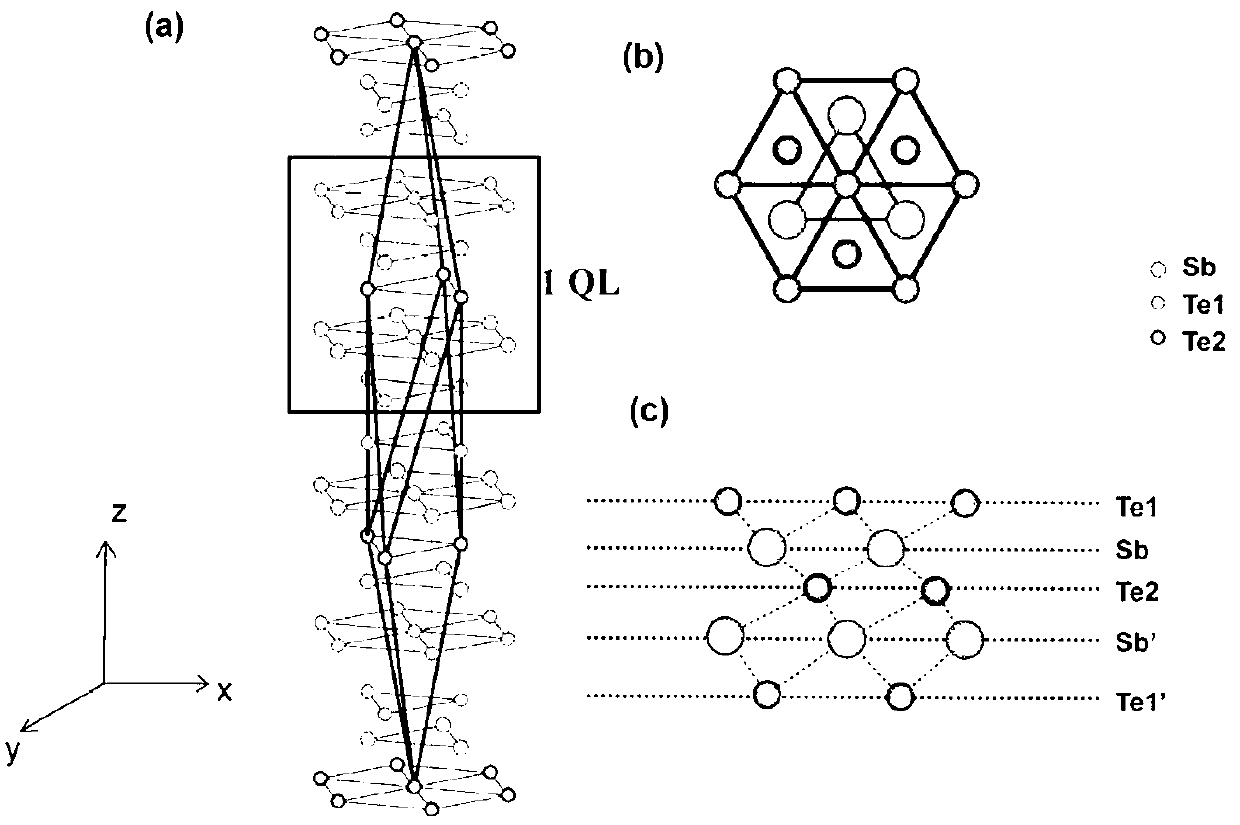
[0070] The magnetic doped topological insulator quantum well film is Cr 0.15 (Bi 0.10 Sb 0.9 ) 1.85 Te 3 , the thickness is 5QL, and the insulating substrate 30 is an STO substrate.
[0071] The Hall curves of the topological insulator structure under different back gate voltages were measured. see Figure 6-9 , at a temperature of 30 milliKelvin (mK), the R of the sample AH With the back gate voltage (V b ) changes with changes. Figure 6-9 Hysteresis also appears in the middle Hall curve, and the sample has very good ferromagnetism. When 0V≤V b ≤10V, the R of the sample AH With V b The change is small when V b at -4.5V, R AH is 25.8 kΩ. where μ 0 H in H is the magnetization, and μ 0 is the vacuum magnetic permeability, and the unit T is Tesla.
Embodiment 2
[0072] Example 2 (T=1.5K, 4QL sample, back gate regulation)
[0073] The magnetic doped topological insulator quantum well film is Cr 0.22 (Bi 0.22 Sb 0.78 ) 1.78 Te 3 , the thickness is 4QL, and the insulating substrate 30 is an STO substrate.
[0074] see Figure 10 , at T=1.5K, 4QL Cr on STO(111) substrate 0.22 (Bi 0.22 Sb 0.78 ) 1.78 Te 3 different V b The Hall curve under Figure 10 shown. from Figure 10 It can be seen that the Hall curve has hysteresis, and the shape of the hysteresis loop is very "square", indicating that the sample has very good ferromagnetism. by V b regulation, can obtain higher R AH . R AH With V b The increase first increases and then decreases, when V b =45V, R AH It reaches the maximum, about 10 kΩ, which is close to 0.4 quantum resistance (25.8kΩ). Figure 11 is the sample at different V b under the reluctance curve for different V b Below, the magnetoresistance curves are all "butterfly-shaped", which also shows that t...
Embodiment 3
[0075] Example 3 (T=100mK, 4QL sample, back gate regulation)
[0076] The magnetic doped topological insulator quantum well film is Cr 0.22 (Bi 0.22 Sb 0.78 ) 1.78 Te 3 , the thickness is 4QL, and the insulating substrate 30 is an STO substrate.
[0077] The Hall curves of the topological insulator structure under different back gate voltages were measured. see Figure 13 , at a temperature of 100 milliKelvin (mK), the R of the sample AH With the back gate voltage (V b ) changes with changes. Figure 13 Hysteresis also appears in the middle Hall curve, and the sample has very good ferromagnetism. When 0V≤V b ≤20V, the R of the sample AH With V b little change in R AH Close to 0.6 quantum resistance (25.8kΩ). Specifically, when V b =10 V, R AH max, (R AH ) max =0.59h?e -2 , that is about 15.3kΩ. This value has far exceeded half of the quantum Hall resistance value, and is the largest abnormal Hall resistance that can be obtained in the world so far. Fi...
PUM
Abstract
The invention relates to a preparation method of a topological insulator structure, which comprises the following steps of: providing a strontium titanate substrate; performing thermal treatment on the strontium titanate substrate in a molecular beam epitaxial reaction cavity so that the surface is clean; heating the strontium titanate substrate and forming beams of Bi, Sb, Cr and Te in the molecular beam epitaxial reaction cavity at the same time; and controlling the flow of the beams of Bi, Sb, Cr and Te to control the proportion of Bi, Sb, Cr to Te so that a hole-type carrier introduced into a magnetic doping topological insulator quantum well film and an electronic type carrier introduced into the magnetic doping topological insulator quantum well film basically cancel out each other, thus a magnetic doping topological insulator quantum well film is formed on the surface of the strontium titanate substrate, wherein the material of the magnetic doping topological insulator quantum well film is expressed by a chemical formula Cry(BixSb1-x)(2-y)Te3, 0<x<1, 0<y<2, and the thickness of the magnetic doping topological insulator quantum well film is 3-5QL.
Description
technical field [0001] The invention belongs to the field of condensed matter physics and relates to a preparation method of a topological insulator structure. Background technique [0002] The Hall effect (HE) was discovered by American physicist E. H. Hall in 1879 while studying the conductive structure of metals. When the current passes through the conductor perpendicular to the external magnetic field, a potential difference will appear between the two end faces of the conductor perpendicular to the direction of the magnetic field and current. This phenomenon is the Hall effect. Scientists subsequently discovered the anomalous Hall effect (AHE) in magnetic materials and the spin Hall effect (SHE) in semiconductors. Theoretically, the three Hall effects should exist in their corresponding quantized forms under certain conditions. In 1980, German physicist K. V. Klitzing discovered the quantum Hall effect (quantum Hall effect, QHE) (Klitzing K. V. et al., New Method for...
Claims
Application Information
Patent Timeline
Application Date:The date an application was filed.
Publication Date:The date a patent or application was officially published.
First Publication Date:The earliest publication date of a patent with the same application number.
Issue Date:Publication date of the patent grant document.
PCT Entry Date:The Entry date of PCT National Phase.
Estimated Expiry Date:The statutory expiry date of a patent right according to the Patent Law, and it is the longest term of protection that the patent right can achieve without the termination of the patent right due to other reasons(Term extension factor has been taken into account ).
Invalid Date:Actual expiry date is based on effective date or publication date of legal transaction data of invalid patent.

