Bulk conductive microchannel plate

A technology of micro-channel plate and micro-channel, which is applied in the directions of dynode, electron multiplier details, multiple dynode electrode devices, etc. It can solve problems such as high noise, affecting signal image clarity, and unsatisfactory performance and structure technology. , to achieve the effect of prolonging service life, excellent signal gain effect, extreme electronic gain and signal-to-noise ratio

Inactive Publication Date: 2013-03-27
CHANGSHU XINLI MAGNETIC IND
View PDF10 Cites 6 Cited by
  • Summary
  • Abstract
  • Description
  • Claims
  • Application Information

AI Technical Summary

Problems solved by technology

[0003] With regard to the material of the microchannel plate in the prior art: usually make with lead silicate glass (as CN101913765A " be used to make microchannel plate glass matrix Glass"), it has the following disadvantages: First, because the glass itself is an insulator and does not conduct electricity, it must be heated and reduced in hydrogen to form a conductive layer on the surface of the microchannel to transport electrons to supplement the surface of the channel wall. Electrons strike "secondary electrons" that are continuously emitted outward
[0004] As far as the physical mechanism of the microchannel plate in the prior art is concerned: due to the large noise and easy aging, the operating voltage cannot be too high (only 800-1000 volts), The gain is limited (the gain is 10 3 -10 4 ); if you try to increase the gain by increasing the voltage, on the one hand, the noise will increase and affect the signal, on the other hand Speeding up the aging of the microchannel plate shortens the working life
[0005] As far as the structure of the microchannel plate in the prior art is concerned: due to the lack of performance, the structure (and process) is not ideal
One of the reasons is that because it is made of lead silicate glass, if it is used for extreme ultraviolet single photon counting detectors such as the detection camera used to make the Chang'e satellite's detection of the ionosphere radiation signal of the earth's atmosphere, it needs to be processed in a vacuum. The micro-channel plate is heated and degassed for a long time, and the working channel of the micro-channel plate is washed with electrons several times to reduce noise and improve the signal-to-noise ratio of weak signals in the universe. In particular, it is necessary to combine at least two (two) micro-channel plates Superimposed use; the reason why two or more microchannel plates need to be superimposed is that the length-to-diameter ratio of a single microchannel is small, usually around 1:40 (the ratio of diameter to length is 1:40), making it difficult to Satisfies the requirement of a gain of 10 6 or higher for detection of extremely weak signals such as single photon counting devices, and practice has proved that two or more prior art microchannel plates are stacked and connected in series under voltage Work (in order to increase the gain) will have the following disadvantages: In addition to the high noise of the micro-channel plate itself, the signal electrons in the gap between the superimposed micro-channels will cause additional noise due to scattering, affecting signal reception and image acquisition clarity of

Method used


Image

  • Bulk conductive microchannel plate
  • Bulk conductive microchannel plate
  • Bulk conductive microchannel plate

Examples


Embodiment 1

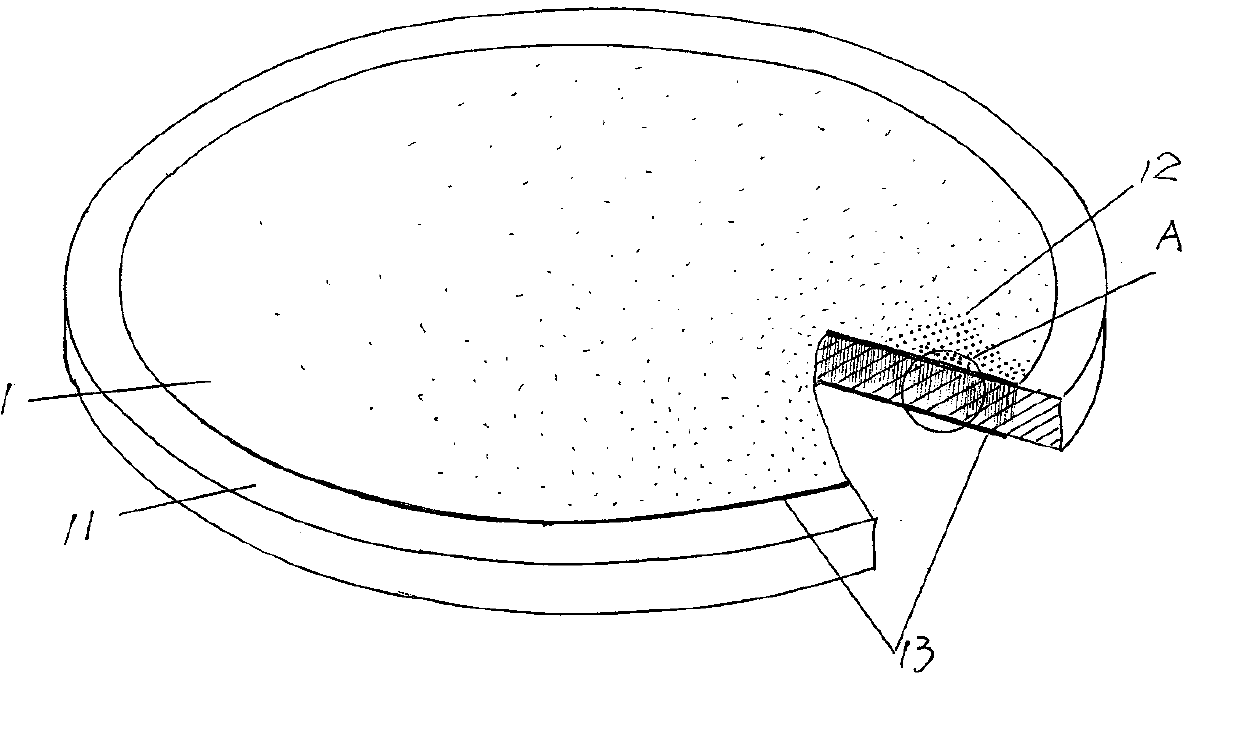
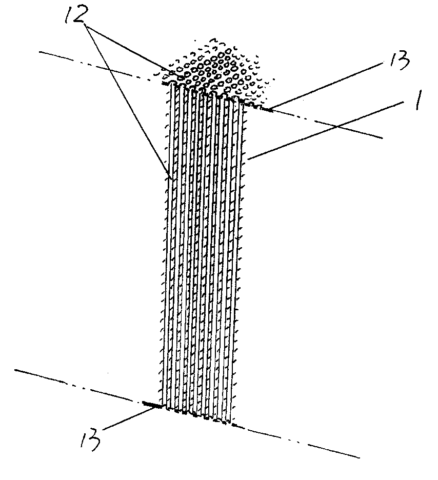
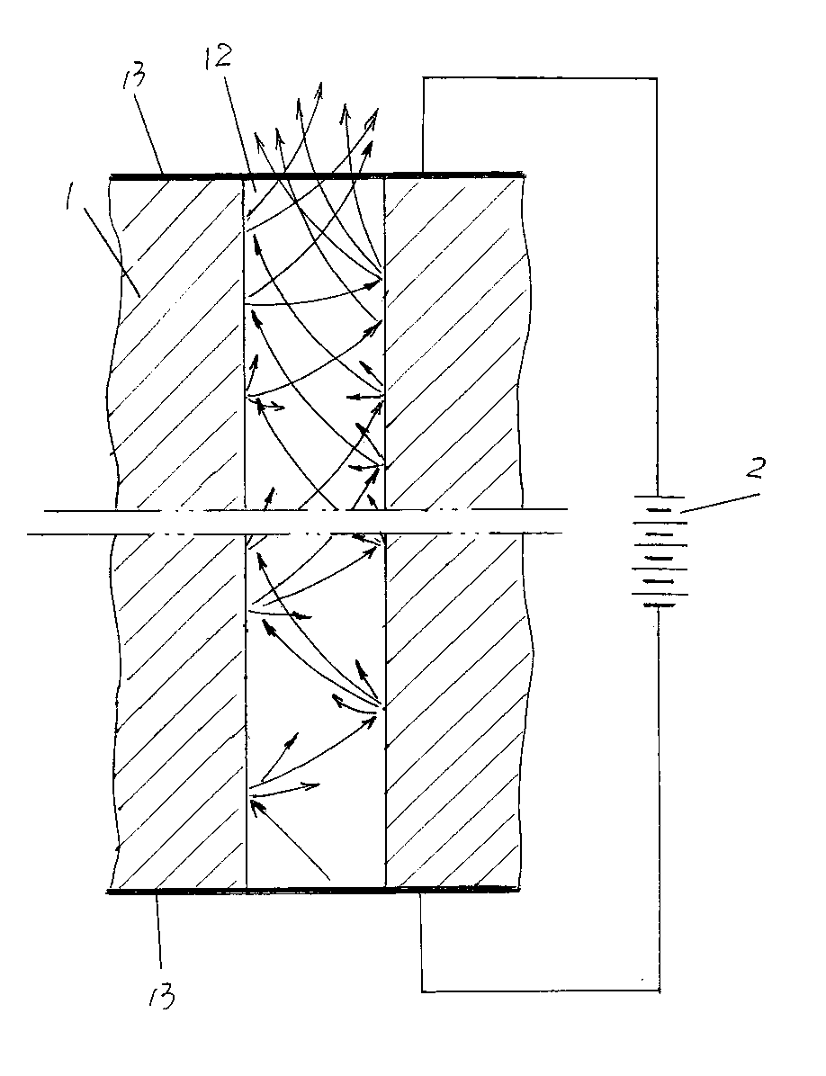
[0032] See figure 1 and figure 2, a plate-shaped glass substrate 1 is provided. Although the shape of the plate-shaped glass substrate 1 shown in the figure is a disc shape, it is not limited to this shape. For example, it can also be made into a rectangular shape. In this glass substrate 1 The edge positions on both sides and the positions corresponding to each other respectively constitute a solid annular glass edge 11, the width of the annular glass edge 11 is 2-3mm, on the glass substrate 1 and in the area inside the annular glass edge 11 In a dense state, there are micro-channels 12 penetrating from one side of the glass substrate 1 to the other side, and a metal coating layer is coated on both sides of the glass substrate 1 and also in the region of the solid ring-shaped glass edge 11 13.

[0033] As the technical gist of the technical solution provided by the present invention, the aforementioned glass substrate 1 is a semiconductor glass substrate, and the volume re...

Embodiment 2

[0037] Only change the thickness of the glass substrate 1, that is, the semiconductor glass, to 0.22 mm, and the volume resistance of the semiconductor glass substrate, that is, the semiconductor glass, to 10 9 Ω, the operating voltage is changed to 1400 volts, the ratio of the diameter and length of the microchannel 12 is 1:80, so the diameter of the microchannel 12 is 2.75 μm, and the electronic gain of the microchannel 12 is 10 6 , the thickness of the metal coating layer 13 is changed to 200 nm, and the width of the annular glass edge 11 is 3 mm. Change the ratio of the molecular formula weight percentage of the semiconductor glass, that is, the semiconductor glass matrix, to: P 2 o 5 55%, V 2 o 5 14%, FeO 4%, WO 3 6%, Sb 2 o 3 3% and PbO18%. All the other are the same as the description to embodiment 1.

Embodiment 3

[0039] Only change the thickness of the glass substrate 1, that is, the semiconductor glass, to 0.21 mm, the operating voltage to 1200 volts, the ratio of the diameter to the length of the microchannel 12 to 1:70, and the electronic gain of the microchannel 12 to 10 5 , the thickness of the metal coating layer 13 is changed to 100 nm, the diameter of the microchannel 12 is 3 μm, and the width of the annular glass edge 11 is 2.5 mm. Change the chemical composition of semiconductor glass according to the percentage ratio of molecular formula to: P 2 o 5 40%, V 2 o 5 20%, FeO 2%, WO 3 20%, Sb 2 o 3 2% and PbO16%. All the other are the same as the description to embodiment 1.


PUM


Abstract

The invention relates to a bulk conductive microchannel plate, which belongs to the technical field of semiconductor electron multiplication devices. The bulk conductive microchannel plate comprises a platy glass base body; each of the edge parts of two side surfaces of the glass base body forms a solid annular glass side; a microchannel penetrating from one side surface of the glass base body to the other side surface of the glass base body is formed at an area positioned inside the annular glass side; a metal coating film layer is coated on both side surfaces of the glass base body at the area positioned inside the annular glass side; the bulk conductive microchannel plate is characterized in that the glass base body is semiconductor glass; the ratio of the diameter of the microchannel to the length of the microchannel is 1: 60 to 1: 80; and the electron gain of the microchannel is 104-106. The bulk conductive microchannel plate has the advantages of obtaining ideal electron gain, prolonging the service life, ensuring excellent signal gain effect and being excellent in electron gain and noise-signal ratio; and countermovement of positive ions when working is prevented.

Description

technical field [0001] The invention belongs to the technical field of semiconductor electron multiplier devices, and in particular relates to a bulk conductance microchannel plate. Background technique [0002] Microchannel plate (English name: Microchannel Plate, abbreviated as: MCP) is a photomultiplier element made of glass fiber. After a certain voltage is applied to both sides of the microchannel plate, an axial electric field will be generated in the microchannel. , so that each electron or photon entering the channel, that is, the microchannel, collides with the channel wall and generates secondary electrons. The secondary electrons are continuously accelerated under the action of the axial electric field, and then collide with the channel wall to generate more new secondary electrons. Electronics, so that as the process is repeated, electronic gain is generated at the output to enhance the signal, and the weak electronic image or signal can be evenly amplified to mo...

Claims


Application Information

Patent Timeline
Patent Type & Authority Applications(China)
IPC IPC(8): H01J43/22H01J43/24
Inventor 王荣杰易家良潘守芹曾欲强
Owner CHANGSHU XINLI MAGNETIC IND
Why Eureka
Try Eureka