Bulk conductive microchannel plate
A micro-channel plate and micro-channel technology, which is applied to dynodes, detailed information of electron multipliers, electrode devices with multiple dynodes, etc., can solve the problems of unsatisfactory performance, structure and process, affecting signal image clarity, and high noise. Achieve excellent signal gain, avoid overheating and prolong service life
- Summary
- Abstract
- Description
- Claims
- Application Information
AI Technical Summary
Problems solved by technology
Method used
Image
Examples
Embodiment 1
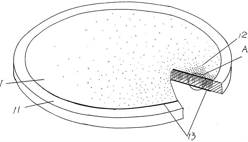
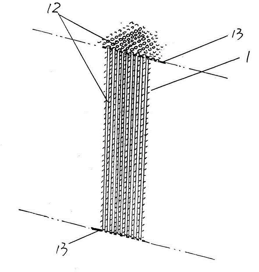
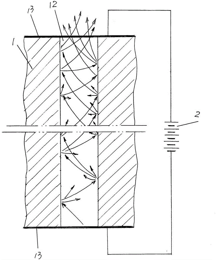
[0032] See figure 1 and figure 2 , a plate-shaped glass substrate 1 is provided. Although the shape of the plate-shaped glass substrate 1 shown in the figure is a disc shape, it is not limited to this shape. For example, it can also be made into a rectangular shape. In this glass substrate 1 The edges of both sides and the positions corresponding to each other are respectively formed with a solid annular glass edge 11, the width of the annular glass edge 11 is 2-3mm, on the glass substrate 1 and in the area inside the annular glass edge 11 In a dense state, there are microchannels 12 penetrating from one side of the glass substrate 1 to the other side, and a metal coating layer is coated on both sides of the glass substrate 1 and also in the region of the solid ring-shaped glass edge 11 13.
[0033] As the technical gist of the technical solution provided by the present invention, the aforementioned glass substrate 1 is a semiconductor glass substrate, and the volume ...
Embodiment 2
[0037] Only change the thickness of the glass substrate 1, that is, the semiconductor glass, to 0.22 mm, and the volume resistance of the semiconductor glass substrate, that is, the semiconductor glass, to 10 9 Ω, the operating voltage is changed to 1400 volts, the ratio of the diameter and length of the microchannel 12 is 1:80, so the diameter of the microchannel 12 is 2.75 μm, and the electronic gain of the microchannel 12 is 10 6 , the thickness of the metal coating layer 13 is changed to 200 nm, and the width of the annular glass edge 11 is 3 mm. Change the ratio of the molecular formula weight percentage of the semiconductor glass, that is, the semiconductor glass matrix, to: P 2 O 5 55%,V 2 O 5 14%, FeO 4%, WO 3 6%, Sb 2 O 3 3% and PbO18%. All the other are the same as the description to embodiment 1.
Embodiment 3
[0039] Only change the thickness of the glass substrate 1, that is, the semiconductor glass, to 0.21 mm, the operating voltage to 1200 volts, the ratio of the diameter to the length of the microchannel 12 to 1:70, and the electronic gain of the microchannel 12 to 10 5 , the thickness of the metal coating layer 13 is changed to 100 nm, the diameter of the microchannel 12 is 3 μm, and the width of the annular glass edge 11 is 2.5 mm. Change the chemical composition of semiconductor glass according to the percentage ratio of molecular formula to: P 2 O 5 40%,V 2 O 5 20%, FeO 2%, WO 3 20%, Sb 2 O 3 2% and PbO16%. All the other are the same as the description to embodiment 1.
PUM
 Abstract
Description
Claims
Application Information


