Method for manufacturing double-faced epitaxial growth GaAs triple-junction solar cell

A solar cell and epitaxial growth technology, applied in the field of solar cells, can solve problems such as unstable cell performance, increased cell manufacturing costs, and compatibility of triple-junction solar cells, and achieve the goals of improving photoelectric conversion efficiency, simplifying the manufacturing process, and improving production efficiency Effect

Active Publication Date: 2013-03-27
TIANJIN LANTIAN SOLAR TECH +2
View PDF4 Cites 10 Cited by
  • Summary
  • Abstract
  • Description
  • Claims
  • Application Information

AI Technical Summary

Problems solved by technology

However, since the solar cell technology of reverse epitaxial growth not only requires a support for secondary layer transfer, but also uses wafer bonding and film substrate lift-off techniques that are non-standard III-V solar cell processes, these Non-standard III-V sola

Method used


Image

  • Method for manufacturing double-faced epitaxial growth GaAs triple-junction solar cell

Examples


Embodiment

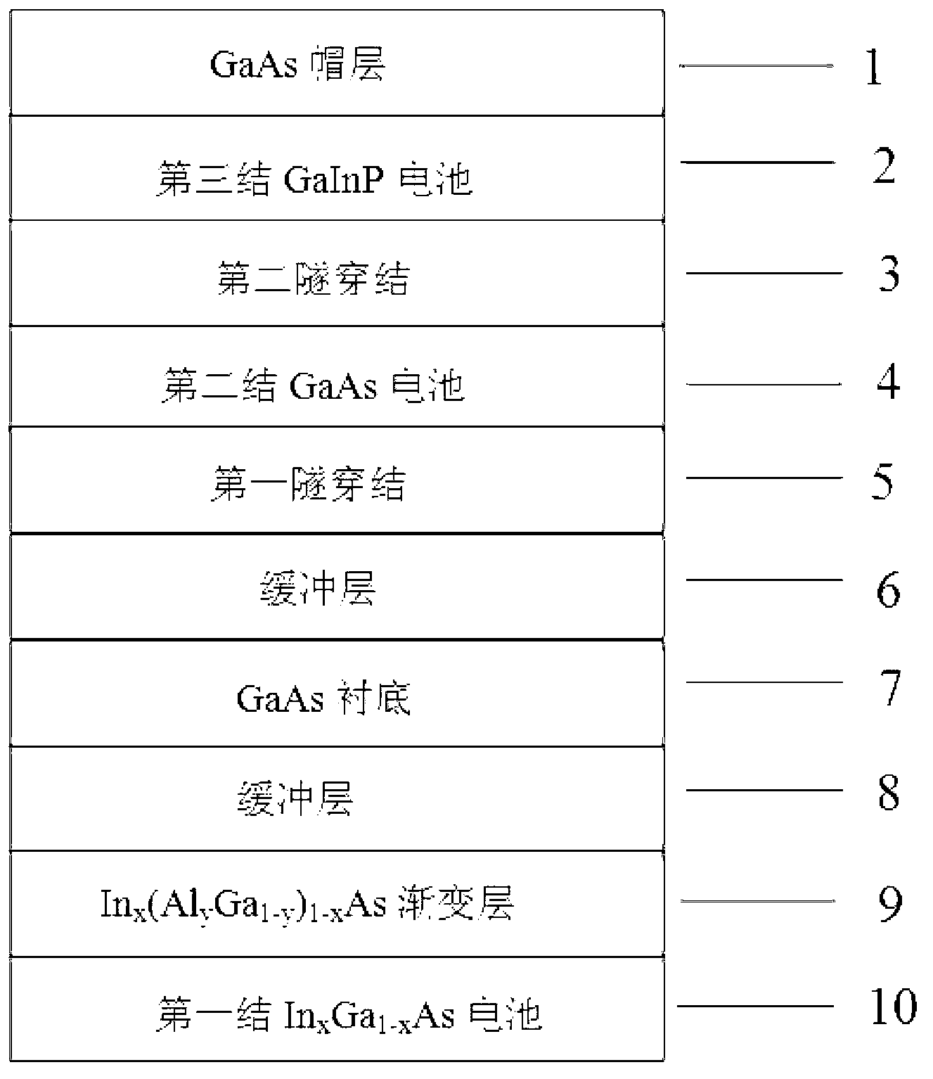
[0020] See attached figure 1 , the preparation method of double-sided epitaxial growth GaAs triple-junction solar cell of the present invention comprises the following preparation steps:

[0021] Step 1. Select the doping concentration as 1×10 18 cm -3 1. An n-type doped GaAs sheet with a thickness of 600 microns is used as the GaAs substrate 7;

[0022] Step 2. Prepare the MOCVD equipment, place the GaAs substrate in step 1 with one side up into the MOCVD operating room, set the growth temperature to 600°C, and epitaxially grow n-type doped GaAs buffer layers 8, n on the GaAs substrate in sequence. Type doped In x (Al y Ga 1-y ) 1-x As gradient layer 9 and the first junction In x Ga 1-x As battery 10;

[0023] The doping concentration of the GaAs buffer layer is 1×10 18 cm -3 , with a thickness of 0.2 microns;

[0024] The In x (Al y Ga 1-y ) 1-x In the As gradient layer, 0.03≤x≤0.3, 0.5≤y≤0.7, the doping concentration is 1×10 19 cm -3 , with a thickness of ...


PUM

PropertyMeasurementUnit
Thicknessaaaaaaaaaa
Doping concentrationaaaaaaaaaa
Thicknessaaaaaaaaaa

Abstract

The invention relates to a method for manufacturing a double-faced epitaxial growth GaAs triple-junction solar cell. The method includes sequentially forming a GaAs buffer layer, an In<x>(Al<y>Ga<1-y>)<1-x>As gradient layer and a first-junction In<x>Ga<1-x>As cell on one face of a GaAs substrate in an epitaxial growth manner; and sequentially forming a GaAs buffer layer, a first tunnel junction, a second-junction GaAs cell, a second tunnel junction, a third-junction GaInP cell and a GaAs cap layer on the other face of the GaAs substrate in an epitaxial growth manner. The GaAs substrate is turned over to be subjected to double-faced epitaxial growth, so that influence of dislocation due to isolation lattice mismatch to the first-junction cell and the second-junction cell which are grown on the back face of the substrate is avoided, the photovoltaic conversion efficiency of the cell is improved, the stable performance of the cell is guaranteed, a process for manufacturing cell is simplified, the manufacturing cost of the cell is lowered, the cell production efficiency is improved, and mass production is easy to implement.

Description

technical field [0001] The invention belongs to the technical field of solar cells, in particular to a method for preparing double-sided epitaxially grown GaAs triple-junction solar cells. Background technique [0002] In solar cells, the improvement of photoelectric conversion efficiency is always the goal that people are constantly pursuing. The current standard InGaP / GaAs / Ge triple-junction solar cell technology with a photoelectric conversion efficiency of 41.6% can no longer meet people's further needs. In order to further improve the photoelectric conversion efficiency of solar cells, people continue to develop technologies based on standard InGaP / GaAs / Ge triple-junction solar cells. It has been found through research that the reverse epitaxial growth of III-V solar cells has become another important technology to improve photoelectric conversion efficiency, that is, through a secondary layer transfer support, wafer bonding and substrate lift-off techniques are used. ...

Claims


Application Information

Patent Timeline
IPC IPC(8): H01L31/18
CPCY02P70/521Y02P70/50
Inventor 王帅高鹏刘如彬康培孙强穆杰
Owner TIANJIN LANTIAN SOLAR TECH
Why Eureka
Try Eureka