

Preparation method of gallium arsenide thin-film multijunction stacked solar cells
A technology of solar cells and gallium arsenide, applied in the field of solar cells, can solve problems such as lattice mismatch, increase cell cost, and affect photoelectric conversion efficiency.
- Summary
- Abstract
- Description
- Claims
- Application Information
AI Technical Summary
Problems solved by technology
Method used
Image

Examples
Embodiment
[0044] Example: see attached Figure 1-Figure 5 :
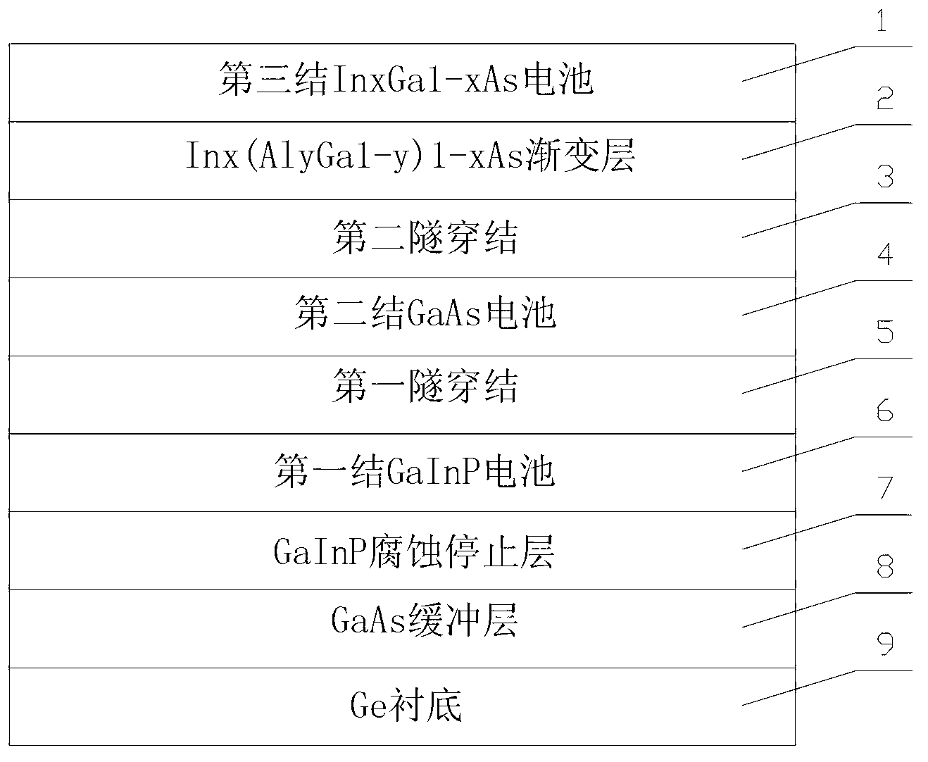
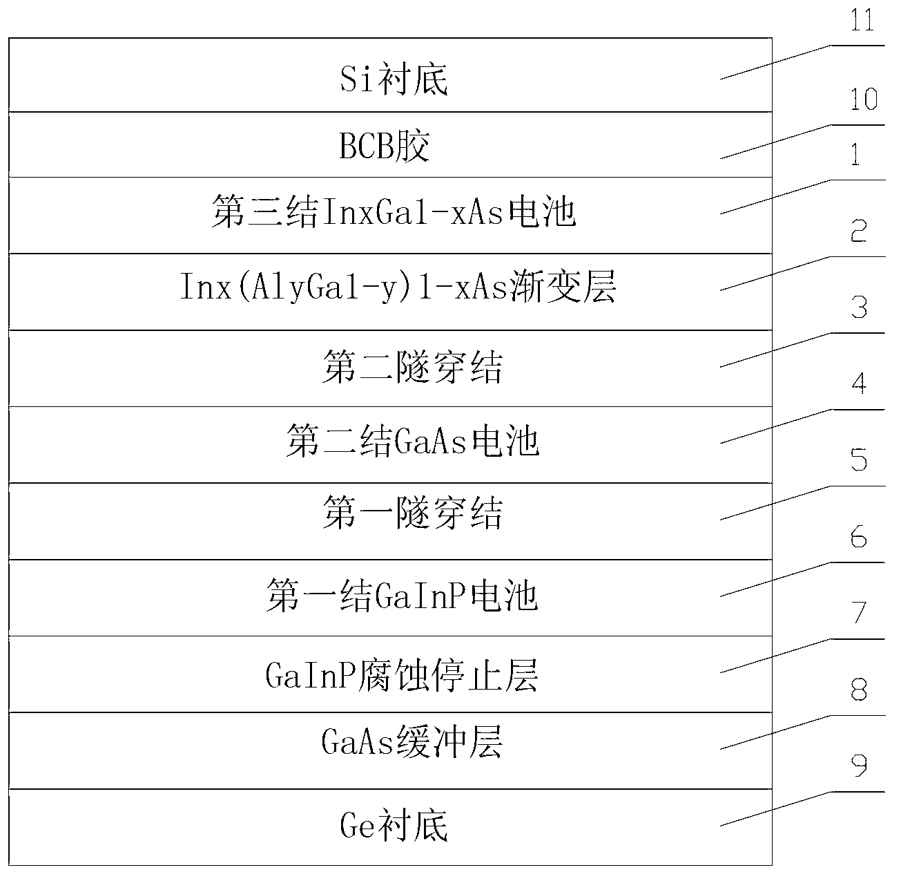
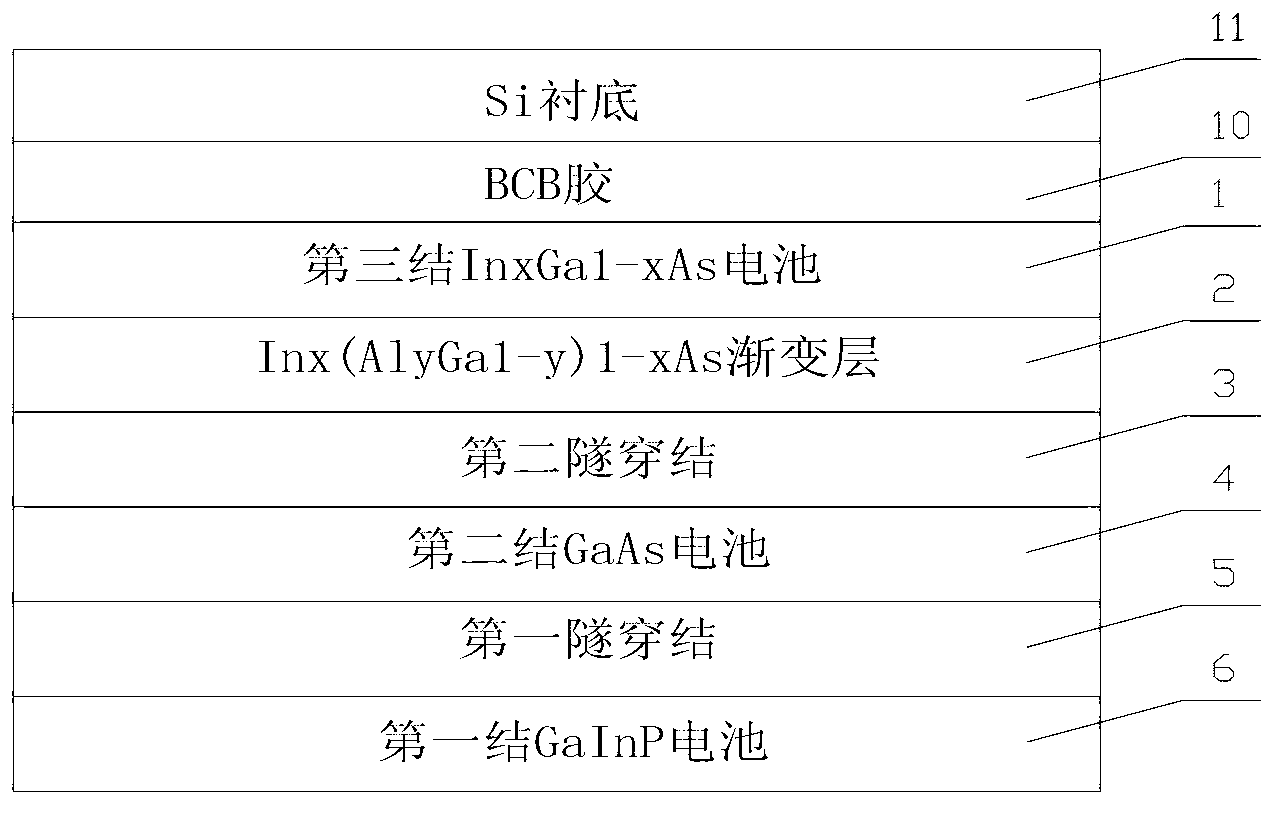
[0045] Step 1. Reverse growth of epitaxial layer to prepare GaAs triple-junction solar cell
[0046] (1) select an n-type doped Ge sheet as the Ge substrate 9, the thickness of the Ge sheet is 150-200 microns (the preferred thickness of the present invention is 150 microns), and the doping concentration is 1×10 17 -1×10 18 cm -3 (the preferred doping concentration of the present invention is 1×10 18 cm -3 );
[0047](2) MOCVD equipment is used to epitaxially grow a GaAs buffer layer 8, a GaInP corrosion stop layer 7, an n-type doped GaAs cap layer, a first junction GaInP cell 6 as a top cell, and a first tunnel cell on the Ge substrate in (1) in sequence. Punch junction 5, second junction GaAs battery 4 as middle battery, second tunnel junction 3, n-type doped In x (Al y Ga 1-y ) 1-x As graded layer 2 and the third junction In as the bottom cell x Ga 1-x As battery 1, the growth temperature is 500°C-800°C (the pre...
PUM
| Property | Measurement | Unit |
|---|---|---|
| Thickness | aaaaa | aaaaa |
| Thickness | aaaaa | aaaaa |
| Thickness | aaaaa | aaaaa |
Abstract
Description
Claims
Application Information