

Liquid crystal display device, polysilicon array substrate and manufacturing method
The technology of an array substrate and a manufacturing method, which is applied in the field of liquid crystal display devices, can solve the problems of high manufacturing cost and complicated manufacturing process of the display panel, and achieve the effects of improving the display effect, simplifying the interlayer structure, and reducing the manufacturing cost
- Summary
- Abstract
- Description
- Claims
- Application Information
AI Technical Summary
Problems solved by technology
Method used
Image

Examples
specific Embodiment approach
[0045] As a specific embodiment of the present invention, a method for manufacturing an array substrate is used to form the above-mentioned top-gate TFT polysilicon array substrate, such as Figure 4 As shown, the method includes:
[0046] Step S1, forming a polysilicon active layer and a pixel electrode.
[0047] It should be noted that, in the present invention, the patterning process includes steps such as glue application, exposure, development, etching, and photoresist stripping.
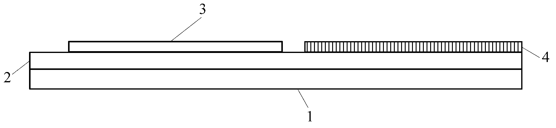
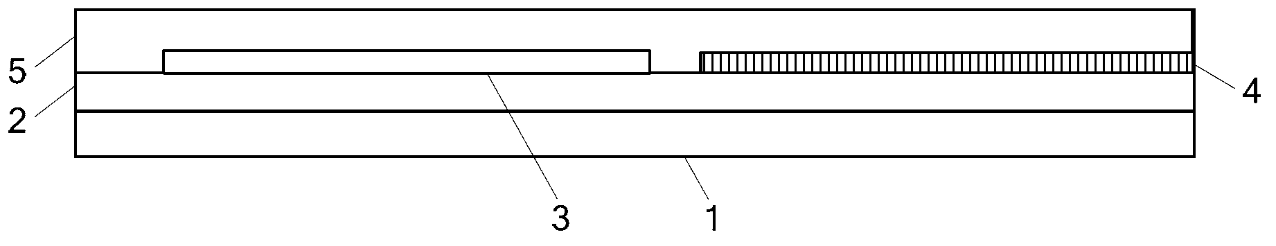
[0048] Specifically, such as Figure 2a As shown, first a buffer layer 2 is formed on the substrate 1, and then an amorphous silicon layer is formed on the buffer layer 2, and the amorphous silicon layer is converted into a polysilicon layer by excimer laser annealing process using low-temperature polysilicon technology. Then, a polysilicon active layer 3 is formed through one patterning process through process steps such as masking, exposure, etching, and photoresist removal. Then, a transp...
Embodiment approach
[0062] As a preferred implementation mode of the present invention, a method for manufacturing an array substrate in this embodiment further includes:
[0063] Step S7, forming a passivation layer on the substrate after step S6, and forming peripheral connection holes through a patterning process.
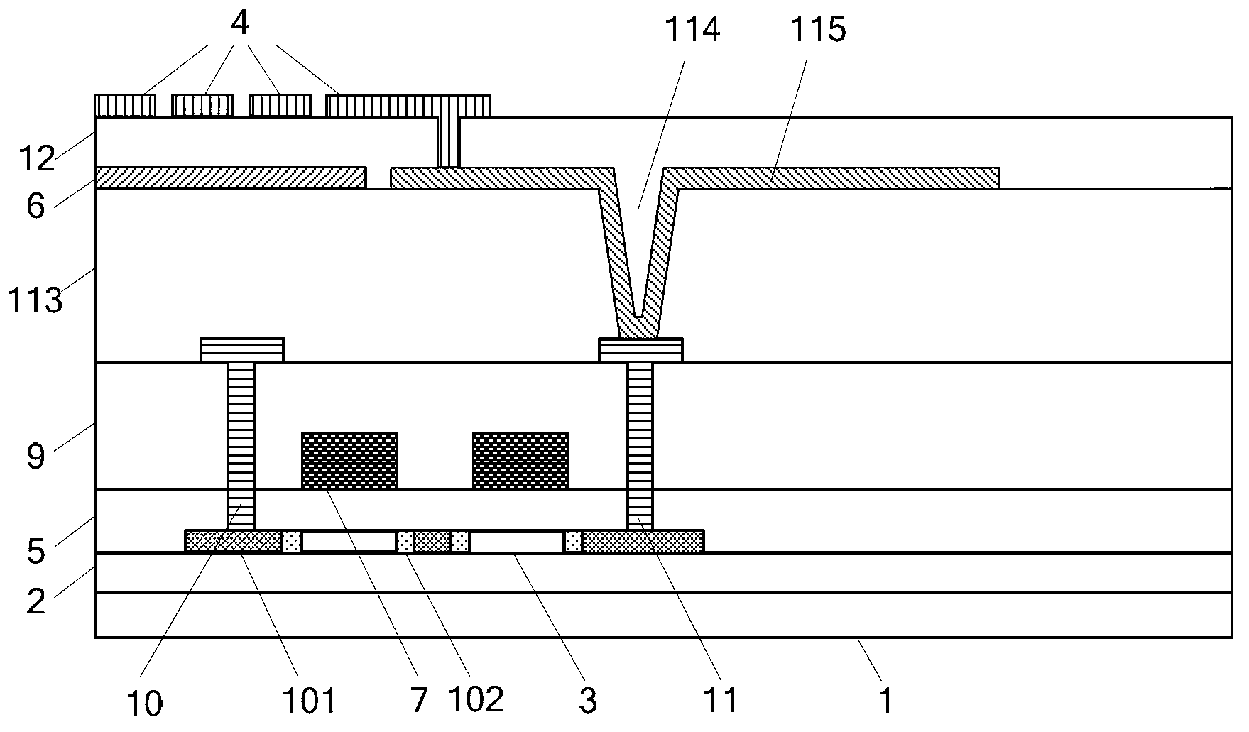
[0064] Specifically, such as Figure 2g As shown, firstly a layer of insulating material is formed on the substrate after step S6 to form a passivation layer 12 . The passivation layer 12 is used to protect structures and devices in the array substrate, and then a peripheral connection hole (not shown) is formed through a patterning process.
[0065] The manufacturing method of the array substrate provided by the present invention saves the organic layer and via structure in the prior art by adjusting the interlayer position of the pixel electrode and the common electrode in the polysilicon array substrate, and simplifies the interlayer structure of the array substrate. The produ...
PUM
 Abstract
Description
Claims
Application Information