Formation method of local air gaps

An air-gap and air-gap technology, applied in the direction of electrical components, semiconductor/solid-state device parts, electric solid-state devices, etc., can solve the problems of photolithography, etching production inconvenience, complex process, etc., to facilitate subsequent production and simplify the formation The effect of craft

Inactive Publication Date: 2013-04-03
SHANGHAI INTEGRATED CIRCUIT RES & DEV CENT
View PDF8 Cites 4 Cited by
  • Summary
  • Abstract
  • Description
  • Claims
  • Application Information

AI Technical Summary

Problems solved by technology

The other is a localized air gap formation method, that is, after the interconnection structure is completed, reverse etching is performed, and the feature of air gaps will be formed when the feature size is small by using the plasma gas deposition method. The size of the place will be completely covered, and each layer of interconnection structure will increase the etching, film deposition, CMP (chemical mechanical polishing) and other processes, and the process is more complicated.
For example, in the US patent US7790601B1, it is a method of local air gaps. By additionally introducing a photolithography mask, photolithography, etching, etc. are performed between wires of a specific size, and the process is relatively complicated.
In addition, since the feature size is already the smallest size on the mask plate, the alignment, photolithography, etching, etc. caused by the additionally introduced photolithography mask will bring inconvenience to subsequent production

Method used


Image

  • Formation method of local air gaps
  • Formation method of local air gaps
  • Formation method of local air gaps

Examples


Embodiment Construction

[0038] The implementation of the present invention will be described in detail below in conjunction with the drawings and examples, so that the realization process of how to use technical means to solve technical problems and achieve technical effects in the present invention can be fully understood and implemented accordingly.

[0039] In the following embodiments of the present invention, the ultra-low dielectric film is combined with the film layer structure formed by the spin-on dielectric film, and on this basis, the first metal layer and the second metal layer and the through hole between the two layers of metal are formed. The interconnection structure is then etched and the ultra-low dielectric material is deposited to form an air gap.

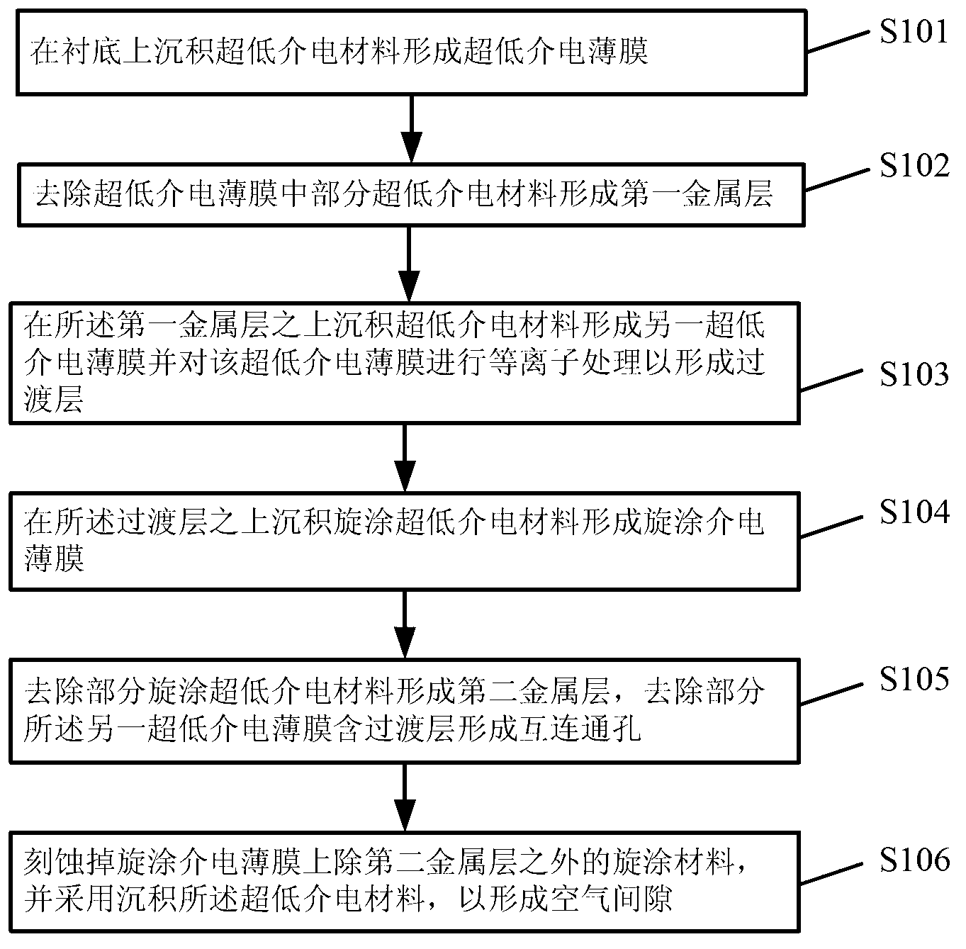
[0040] figure 1 It is a flow chart of the method for forming a local air gap in Embodiment 1 of the present invention, as figure 1 As shown, in this embodiment, the method for forming the local air gap may include:

[0041] Step S101...


PUM

PropertyMeasurementUnit
thicknessaaaaaaaaaa
thicknessaaaaaaaaaa
thicknessaaaaaaaaaa

Abstract

The invention discloses a formation method of local air gaps. The method includes: depositing ultralow dielectric material on a substrate to form an ultralow dielectric film, and removing part of the ultralow dielectric material to form a first metal layer; depositing ultralow dielectric material on the first metal layer to form another ultralow dielectric film, subjecting the ultralow dielectric film to plasma treatment to obtain a transition layer; depositing spin-coating ultralow dielectric material on the transition layer to form a spin-coating dielectric film, removing part of the spin-coating ultralow dielectric material to form a second metal layer, and removing part of the other ultralow dielectric film with the transition layer to form interconnecting vias; etching to remove the spin-coating material on the dielectric films, except for the part outside the second metal layer, and depositing ultralow dielectric material to form air gaps. The formation process of the local gaps is simplified, and subsequent production is facilitated.

Description

technical field [0001] The invention belongs to the field of semiconductor manufacturing, and in particular relates to a method for forming a local air gap. Background technique [0002] In semiconductor chips such as high-performance processors, microcontrollers and communication chips, etc., it is usually necessary to set up a high-speed interconnection structure in an independent chip to perform different functions such as logic operations, data storage and reading, and control. The provision of signals, etc. It can be seen that the interconnection structure will affect the running speed of the chip to a certain extent. For example, due to the signal delay in the interconnection structure, the running speed of the chip is close to the limit. The signal delay in the interconnection structure is proportional to the RC product of the interconnection structure, R represents the interconnection equivalent resistance of the interconnection lines in the interconnection structur...

Claims


Application Information

Patent Timeline
Patent Type & Authority Applications(China)
IPC IPC(8): H01L21/768H01L23/522
Inventor 胡正军
Owner SHANGHAI INTEGRATED CIRCUIT RES & DEV CENT
Why Eureka
Try Eureka