Printed circuit board with partial housing encapsulated in a pressure-resistant manner

A technology for circuit boards and circuit board assemblies, which is applied in the direction of assembling printed circuits, printed circuits, and printed circuits with electrical components, which can solve the problems of complex manufacturing processes, component failures, and delayed development processes in the potting section.

Inactive Publication Date: 2013-04-03
R STAHL SCHALTGERATE
View PDF12 Cites 1 Cited by
  • Summary
  • Abstract
  • Description
  • Claims
  • Application Information

AI Technical Summary

Problems solved by technology

Mechanical stresses also develop between the potting (Verguss) and the conductor rows (Leiterzug) of the circuit board, which can lead to failure of the component
In addition, the manufacture of the potting part is a complicated manufacturing process
Furthermore, the quality-based identification of potting requires detailed and time-consuming inspections, which delays the development process

Method used


Image

  • Printed circuit board with partial housing encapsulated in a pressure-resistant manner
  • Printed circuit board with partial housing encapsulated in a pressure-resistant manner
  • Printed circuit board with partial housing encapsulated in a pressure-resistant manner

Examples


Embodiment Construction

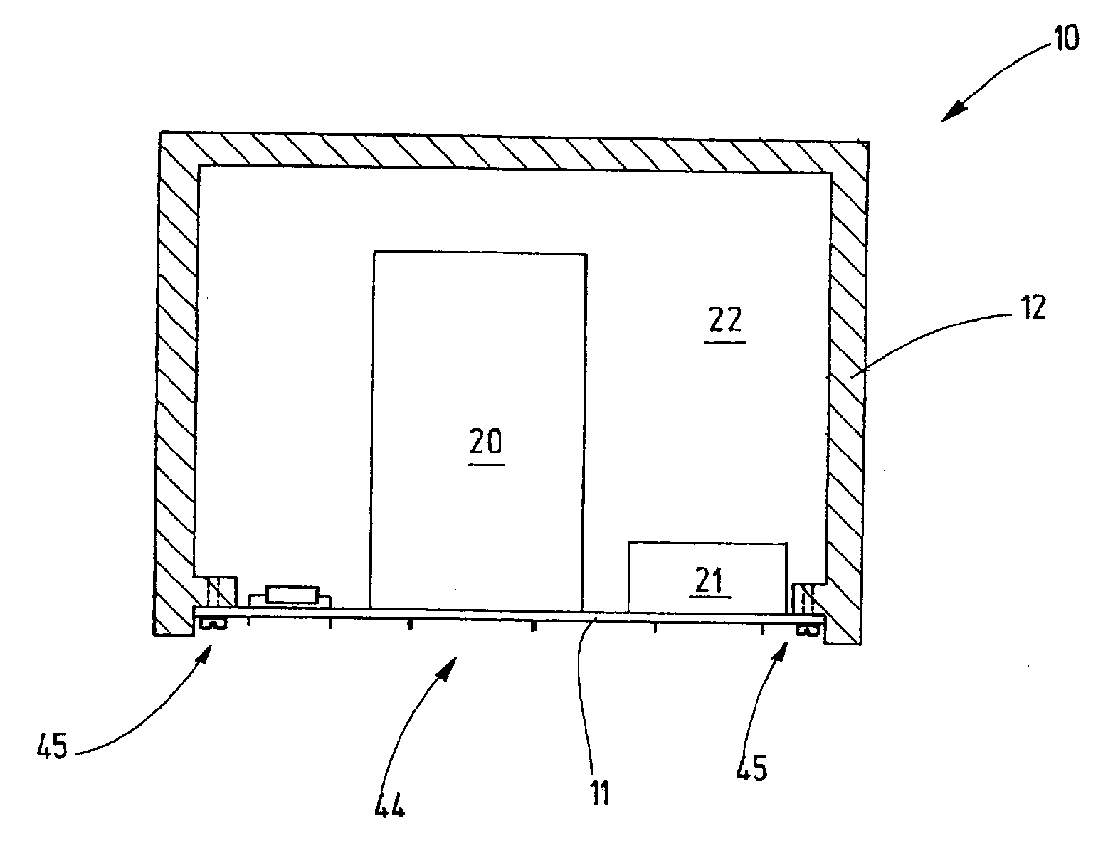
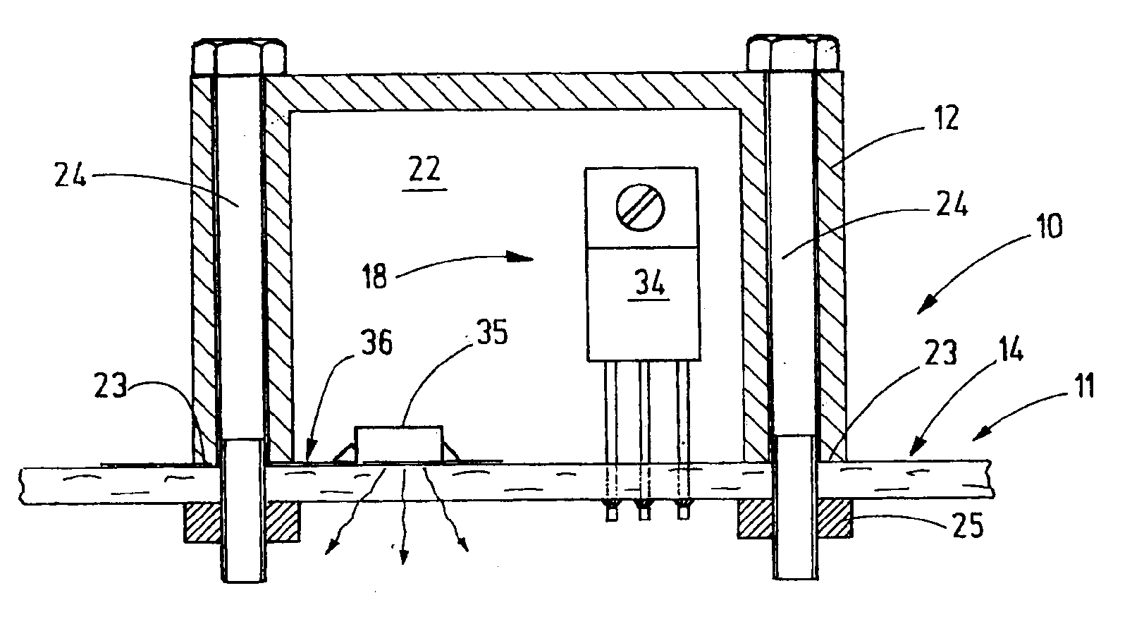
[0029] exist figure 1 A circuit board assembly 10 is illustrated in , to which a circuit board 11 and at least one housing part 12 belong. The circuit board 11 has a plate-shaped carrier (Traeger) 13 with a first flat side 14 and a second flat side 15 (see figure 2 ). The circuit board has columns of conductors. It is arranged, for example, in the carrier 13 . Alternatively or additionally, a conductor row 16 can be arranged on at least one of the two flat sides 14 , 15 . Further conductor rows 17 can be arranged on the respective other flat side.

[0030] Conductor row 16 or 17 forms a non-intrinsically safe line with at least one electrical component 18 . Electrical components 18 may be energy storage components (such as inductors or capacitors), transformers, consumer components (such as resistors), electronic components (such as diodes, Z diodes, transistors, integrated circuits), optoelectronic components (such as light-emitting diodes tube), connecting terminal as...


PUM


Abstract

The invention is suitable for electronic assemblies in regions at risk of explosion, i.e. in regions in which an explosive atmosphere can occur. In this case, non-intrinsically safe circuits can be protected by the electrical components (18) involved being housed by at least one housing part (12) held on the printed circuit board (11), thus giving rise to an Ex-d space. In this case, the printed circuit board can terminate the housing part (12) on one side. Alternatively, a second housing part (26) can be provided, wherein the housing parts (12, 26) then accommodate the printed circuit board (11) between them. In this case, the printed circuit board can serve as a wiring feedthrough and likewise form part of the Ex-d housing. The Ex gap between the printed circuit board (11) and the upper housing part (12) and / or the lower housing part (26) prevents flame flashover.; With the arrangement according to the invention, the potting of non-intrinsically safe electrical circuits or electronic assemblies becomes superfluous. Faults that could occur as a result of stresses between the potting and the printed circuit board or the electrical components (18) are now precluded.

Description

technical field [0001] The invention relates to an explosion-proof printed circuit board assembly (Leiterplattenanordnung). [0002] In particular, the invention relates to electronic assemblies suitable for use in environments where an explosive atmosphere is present at least occasionally, or more frequently, as well. In particular, the invention relates to a printed circuit board assembly with at least one non-intrinsically safe line, that is to say a line in which voltages and currents occur which can lead to ignition of an explosive gas mixture, at least in the event of a fault. Background technique [0003] For explosion protection of electronic devices it is known to install them in a housing which is connected to the ambient air, for example via a sintered metal plate. For this purpose, DE 10 2005 050 914 B4 discloses a gas measuring device with a measuring cell. In the measuring cell there is a thin coiled platinum wire surrounded by small ceramic beads with cataly...

Claims


Application Information

Patent Timeline
Patent Type & Authority Applications(China)
IPC IPC(8): H02B1/28H05K3/34
CPCH02B1/28H05K2201/10409H05K5/02H05K2201/10371H05K1/182
Inventor J.施特里策尔贝格F.弗里
Owner R STAHL SCHALTGERATE
Why Eureka
Try Eureka