Check patentability & draft patents in minutes with Patsnap Eureka AI!

Method for manufacturing large-area nano gap electrode arrays in parallel

A nano-slit electrode and nano-slit technology, which is applied in the field of nano-manufacturing, can solve the problems of complex, time-consuming electrochemical processes, complex technological processes, etc., and achieve the effect of high processing efficiency

Active Publication Date: 2013-04-10
XI AN JIAOTONG UNIV
View PDF6 Cites 11 Cited by
  • Summary
  • Abstract
  • Description
  • Claims
  • Application Information

AI Technical Summary

Problems solved by technology

This method can realize the gap structure with a characteristic scale smaller than 1nm, but this method needs to prepare the original gap structure of tens of nanometers in advance, and also involves complex and time-consuming electrochemical processes in the process of scaling down, and the process is complicated
In addition, electron beam lithography, focused ion beam etching, atomic force probe scribing, scanning tunnel probe scribing and other manufacturing processes can also be used to manufacture nanoscale gap structures, but these serial processing methods can only be used as Laboratory means of nanoslit fabrication, not exploitable as a process method for large-scale manufacturing
[0003] The existing nanoslit tunnel electrode manufacturing methods provide strong support for the research of device principles, but due to various defects in these methods, they cannot be used as a batch processing method.
The manufacture of nanoscale gaps is still a difficult problem to be solved in this kind of nano research field, and it may also be one of the important bottlenecks restricting the industrialization of devices.

Method used


Image

  • Method for manufacturing large-area nano gap electrode arrays in parallel
  • Method for manufacturing large-area nano gap electrode arrays in parallel
  • Method for manufacturing large-area nano gap electrode arrays in parallel

Examples


Embodiment Construction

[0018] The present invention will be described in further detail below in conjunction with the accompanying drawings.

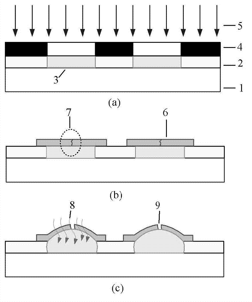
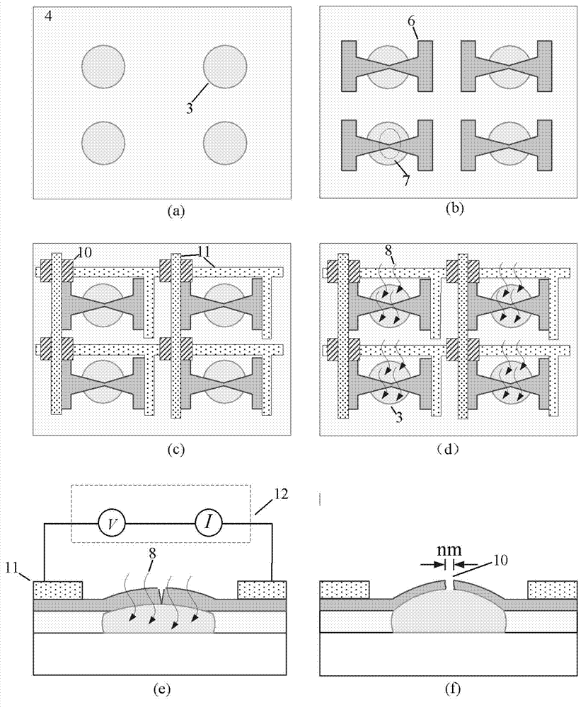
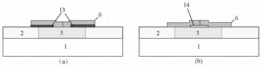
[0019] see figure 1 , a method for parallel fabrication of large-area nanoslit electrode arrays, first using energy beams 5 (ultraviolet light, electron beams, ion beams, and X-rays, etc.) Use the mask plate 4 to carry out beam exposure, after the exposure, PMMA long-bond molecules become short-bond molecules, see figure 1 (a); Then, prepare the metal electrode film 6 on the PMMA photoresist surface, and preset the stress concentration opening 7 at the position where nanoslits need to be produced, for producing stress concentration in the film stretching process, which is easier to generate at the designated position nanoslit, see figure 1 (b); Finally, the short-bond PMMA molecule after exposure absorbs MMA monomer molecule 8 and expands, applying force to the metal film on the upper layer, and the film breaks to produce nano-slit structure 9, see figure ...


PUM

PropertyMeasurementUnit
Thicknessaaaaaaaaaa

Abstract

A method for manufacturing large-area nano gap electrode arrays in parallel comprises the following steps: the graphic structure of a metal film is placed on a PMMA (polymethyl methacrylate) photoresist surface, the PMMA is enabled to be expanded and raised through using the photoexpansion mechanism, the metal film on the PMMA photoresist surface is fractured under the drawing action to produce a nano gap, and the dimension of the structure of the nano gap is regulated and controlled through controlling the raised height of the PMMA.. The nano gap processing method can process all nano gap structure groups with identical dimensions at one time, so that the higher processing efficiency is achieved, meanwhile, expensive equipment and complex processes are not required in the whole process, and the method is suitable for large-quantity and low-cost industrial production, and is a nano gap forming process meeting the manufacturing characteristics of batched production, low cost, consistency and the like.

Description

technical field [0001] The invention relates to the technical field of nano-manufacturing, in particular to a method for parallel manufacturing of large-area nano-slit electrode arrays. Background technique [0002] At present, domestic and foreign researchers have made a lot of explorations on the manufacture of nano-slit structures. The electromigration method is one of the common fabrication methods for nanoslit structures. This method uses the electromigration effect of atoms moving under the action of a large current, and the migration of metal atoms is obtained through the flow of electrons, and finally the nanowires are broken to form nanoslit electrodes. The disadvantage of the electron migration method is that before the preparation of nano-electrodes, ultra-thin nanowires with a characteristic width of tens of nanometers must first be prepared (electron beam lithography and other means are required, and the cost is high). The fusing current is extremely low, thus...

Claims


Application Information

Patent Timeline
IPC IPC(8): B81C1/00B82Y40/00
Inventor 王文君梅雪松刘斌王恪典姜歌东郑卜祥
Owner XI AN JIAOTONG UNIV
Features
  • R&D
  • Intellectual Property
  • Life Sciences
  • Materials
  • Tech Scout
  • Unparalleled Data Quality
  • Higher Quality Content
  • 60% Fewer Hallucinations
Learn More