Reaction chamber for forming tantalum deposition film on silicon substrate, and application thereof

A reaction chamber and silicon substrate technology, applied in the field of reaction chamber, can solve problems such as poor bombardment effect on the side wall of the tantalum ring, cracking and peeling, and excessive particles in the chamber

Active Publication Date: 2013-04-10
SHANGHAI HUALI MICROELECTRONICS CORP
View PDF3 Cites 5 Cited by
  • Summary
  • Abstract
  • Description
  • Claims
  • Application Information

AI Technical Summary

Problems solved by technology

[0003] In the process of depositing tantalum films from tantalum targets by existing machine technology, many tantalum films will be deposited on the tantalum ring, and the bombardment of the surface of the tantalum ring by argon ions can play a certain role in removing the deposited tantalum films. The ion bombardment of the tantalum ring has a certain directionality. The bombardment effect on the side wall and top of the tantalum ring is not good, which will cause the accumulation of the tantalum film in this part. When the tantalum film accumulates to a certain thickness, it will crack and peel off, causing the particles in the cavity to exceed the standard. And other issues

Method used


Image

  • Reaction chamber for forming tantalum deposition film on silicon substrate, and application thereof
  • Reaction chamber for forming tantalum deposition film on silicon substrate, and application thereof

Examples


Embodiment Construction

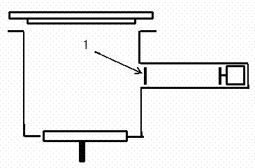
[0015] The invention provides a reaction chamber for a tantalum barrier process, the reaction chamber used for forming a tantalum deposition film on a silicon substrate can reduce the deposition of a tantalum film on a tantalum ring, prevent the film deposited on the tantalum ring from being too thick, and produce The problem of cracking and peeling of tantalum film.

[0016] The reaction chamber for forming a tantalum deposition film on a silicon substrate provided by the present invention will be further described in detail through the following examples, so as to better understand the content of the present invention, but the content of the examples does not limit the scope of the present invention. protected range.

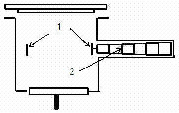
[0017] Such as figure 1 and figure 2 As shown, a cavity is provided on the chamber inner side wall of the reaction chamber body, and a fixed bracket 2 is arranged in the cavity, and the fixed bracket 2 has a telescopic part, and the fixed bracket 2 stretche...


PUM


Abstract

The invention provides a reaction chamber for forming a tantalum deposition film on a silicon substrate, and an application thereof. The reaction chamber comprises a reaction chamber body, wherein an empty cavity is arranged on the inner side wall of the cavity chamber of the reaction chamber body; a fixing bracket is arranged in the empty cavity and is provided with a telescopic component; the fixing bracket extends from the empty cavity under the driving of the telescopic component; and a tantalum ring is arranged at one end, capable of extending from the empty cavity, of the fixing bracket. According to the invention, the depositions of the tantalum film on the tantalum ring are reduced; and the problem of the cracking and the spalling of the tantalum film due to the condition that the film deposited on the tantalum ring is too thick is solved.

Description

technical field [0001] The invention relates to the field of semiconductor manufacturing, in particular to a reaction chamber for forming a tantalum deposition film on a silicon substrate and its application. Background technique [0002] The existing tantalum ring used in the barrier layer of copper interconnection is fixed in the tantalum cavity, and the tantalum ring is ring-shaped. The traditional tantalum barrier process mainly consists of three steps: the first step is the deposition of tantalum nitride and tantalum film. The tantalum material on the tantalum target is mainly deposited on the surface of the silicon wafer, but at the same time the tantalum ring surface is also deposited on the tantalum material. The second step is tantalum reverse sputtering, which mainly uses argon ions to bombard the surface of the silicon wafer and the surface of the tantalum ring. The bombardment of the surface of the silicon wafer can reverse-sputter the tantalum material at the bo...

Claims


Application Information

Patent Timeline
Patent Type & Authority Applications(China)
IPC IPC(8): C23C14/34C23C14/16C23C14/06H01L21/67
Inventor 韩晓刚陈建维张旭昇
Owner SHANGHAI HUALI MICROELECTRONICS CORP
Why Eureka
Try Eureka