Printed circuit board (PCB) chip layout structure and electronic terminal using the same

A chip layout and electronic terminal technology, applied in the direction of printed circuits connected with non-printed electrical components, can solve the space constraints of chip placement and conductive traces, unfavorable engineer layout and conductive traces, and increase the risk of power supply line interference and other issues to achieve the effect of reducing the risk of mutual interference, enhancing electromagnetic compatibility, and shortening the power supply line

Inactive Publication Date: 2013-04-10
共青城赛龙通信技术有限责任公司
View PDF6 Cites 6 Cited by
  • Summary
  • Abstract
  • Description
  • Claims
  • Application Information

AI Technical Summary

Problems solved by technology

Due to the long distance between the CPU and the PMU in this layout structure, the PMU must supply power to the CPU through a long conductive trace, and the increase in the length of the conductive trace will inevitably lead to an increase in the AC and DC impedance of the power supply line between the PMU and the CPU. large, which will inevitably lead to unpredictable voltage drop of the PMU for the core power supply of the CPU, which will have a great impact on the accuracy of the power supply voltage; since the PCB board is also equipped with chips of other modules such as radio frequency, storage, and display, the PMU and the The increase in the length of the power supply conductive traces between the CPUs will inevitably increase the risk of unpredictable interference of the power supply lines by other modules such as radiation and electromagnetic induction, which will have a great impact on the stability of the power supply.
At the same time, the risk of other modules being subjected to electromagnetic interference from the PMU to the CPU core power supply line will also greatly increase, which will seriously affect the performance of other modules; Long power supply conductive traces are connected, which leads to a relatively large restriction on the placement of other module chips and conductive traces on the PCB, which is not conducive to engineers' reasonable layout and conductive traces

Method used


Image

  • Printed circuit board (PCB) chip layout structure and electronic terminal using the same
  • Printed circuit board (PCB) chip layout structure and electronic terminal using the same
  • Printed circuit board (PCB) chip layout structure and electronic terminal using the same

Examples


Embodiment Construction

[0022] The present invention will be further described below in conjunction with the drawings and specific embodiments.

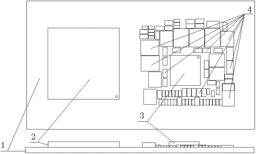
[0023] in figure 1 The CPU 2 and the PMU 3 are arranged on the same side of the PCB 1. The capacitors, inductors, and resistors 4 around the PMU 3 occupy a lot of space, which increases the distance between the CPU 2 and the PMU 3, and electromagnetic interference is easily introduced.

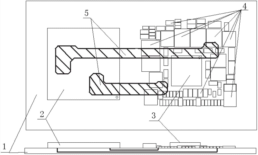
[0024] in figure 2 The conductive trace 5 is connected to the CPU2 and the PMU3, so that the PMU3 supplies power to the CPU2 through the conductive trace 5. It can be seen that the conductive trace 5 is longer, and its AC and DC resistances are large. The power supply is easily unstable and easy to introduce interference.

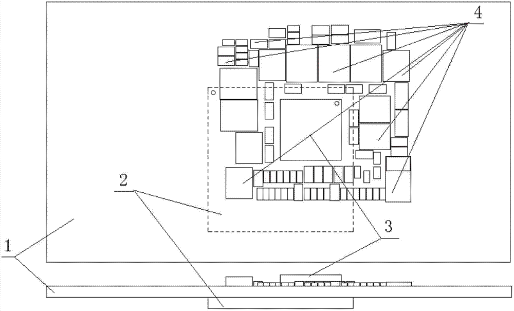
[0025] in image 3 CPU2 is arranged on the back of PMU3 and the projections of the two on the PCB are mostly overlapped, which shortens the distance between CPU2 and PMU3, and at the same time makes full use of the space of PCB1, making the device placement com...


PUM


Abstract

The invention discloses a printed circuit board (PCB) chip layout structure and an electronic terminal using the PCB chip layout structure. The PCB chip layout structure comprises a PCB, a central processing unit (CPU) and a power management unit (PMU). The CPU and the PMU are respectively arranged at two faces of the PCB. The PMU and projection of the CPU on the PCB are partially or completely overlapped. The electronic terminal using the PCB chip layout structure comprises the PCB chip layout structure consisting of the PCB, the CPU and the PMU. The CPU and the PMU are respectively arranged at two faces of the PCB. The PMU and projection of the CPU on the PCB are partially or completely overlapped.

Description

Technical field [0001] The invention belongs to the field of electronic equipment, and particularly relates to the design technology of electronic terminal equipment. Background technique [0002] Generally, electronic terminal equipment contains CPU (central processing unit) and PMU (power management unit) modules. CPU is the computing core and control core device of the terminal. Most commands and data in the terminal must be analyzed and processed by the CPU. It has the functions of interpreting terminal instructions and processing data in the terminal software; while the PMU is the power supply device of the terminal. The power obtained by the terminal from external power supply equipment such as batteries is converted into the voltage value required by each module through the PMU, which is the CPU in the terminal And other modules to provide power; due to the precision of the CPU and its core position in the terminal, the core power of the CPU not only requires accurate volt...

Claims


Application Information

Patent Timeline
Patent Type & Authority Applications(China)
IPC IPC(8): H05K1/18
Inventor 汪小雄
Owner 共青城赛龙通信技术有限责任公司
Why Eureka
Try Eureka