A clean room for semiconductor plant

A clean room and semiconductor technology, applied in the clean room field, can solve the problems of high cost, higher corrosive gas content requirements, large clean room space, etc., and achieve the effect of reducing consumption

Active Publication Date: 2015-08-26
L&K ENG SUZHOU
View PDF5 Cites 1 Cited by
  • Summary
  • Abstract
  • Description
  • Claims
  • Application Information

AI Technical Summary

Problems solved by technology

[0004] In the prior art, there is a direct connection between the production bay and the service area, and since there are a lot of processing equipment in the service area, these processing equipment will generate various waste gases or corrosive gases during the production process. Gas (such as chlorine, hydrogen chloride, etc.), once these corrosive gases overflow, these gases will run into the clean space of the production aisle and the central aisle, so as to directly contact the storage warehouse (Stocker), the placement area (FOUP), and the storage area. The semiconductor products placed in it come into contact, which affects the quality of the product
[0005] In view of the above problems, the method adopted in the prior art is to set a chemical filter in the clean room, but due to the large space in the clean room, it is difficult to completely remove it, and the cost of this method is extremely high; this is necessary for the production of some high-end semiconductors Plants (such as 32 / 28nm high-end process) are very fatal, because high-end semiconductor products have higher requirements for the content of corrosive gases

Method used


Image

  • A clean room for semiconductor plant
  • A clean room for semiconductor plant
  • A clean room for semiconductor plant

Examples


Embodiment 1

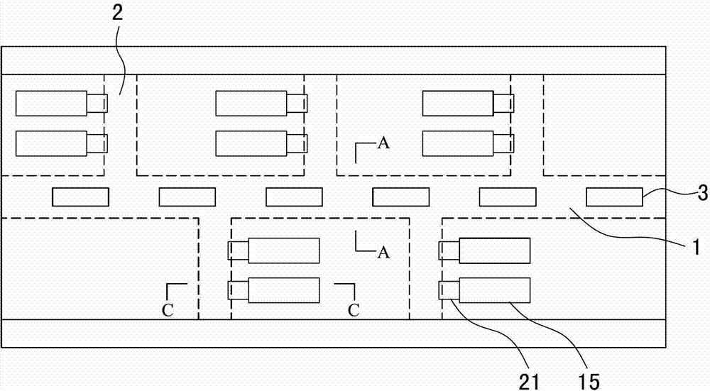
[0037] see Figure 3~8 As shown, a clean room for a semiconductor plant, including a fresh air delivery system, an exhaust system and a large clean space, the large clean space has a central aisle 1 and 5 production aisles 2;

[0038] The large clean space includes a structure space 4, a clean space 5 and a circulation space 6 from top to bottom, a ceiling 7 is provided between the structure space and the clean space, and a raised floor 10 and a concrete slab 11 are provided between the clean space and the circulation space ;

[0039] The central aisle and all the production aisles are surrounded by partitions 8, so that at least a part of the architectural space, the clean space, and the space where the raised floor is located form an independent clean micro-environment structure;

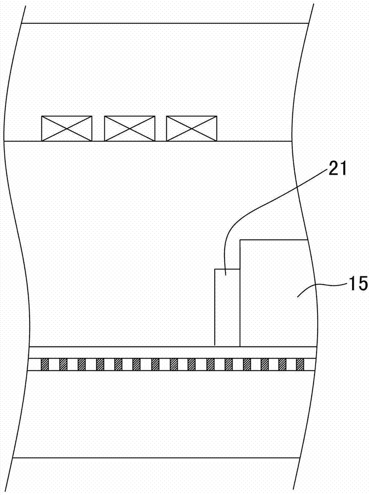
[0040] The bottom of the clean microenvironment is provided with a lower sealing plate 12, and its top is provided with an upper sealing plate 13;

[0041] The inner circumference of the central...


PUM


Abstract

The invention discloses a clean room for a semiconductor plant. The room comprises a fresh air conveying system, an exhaust system and a large clean space, wherein a central pavement and at least one production pavement are arranged in the large clean space, peripheries of the central pavement and the production pavements are provided with baffles, at least one part of frame space, clean space and space of a raised floor form an independent clean micro-environment structure, second baffles are arranged in the central pavement, the second baffles are arranged inside the baffles, the ceiling between the baffles and the second baffles are hollow, and the frame space and the clean space between the baffles and the second baffles form air returning channels. Peripheries of the central pavement and the production pavements are provided with baffles, the independent clean micro-environment structure is formed, and corrosive gas cannot affect storage bins and products in the central pavement and the production pavements.

Description

technical field [0001] The invention relates to a clean room used in a semiconductor workshop, in particular to a production occasion for high-end semiconductors. Background technique [0002] The semiconductor plant is a place specially used to prepare semiconductor devices, and it has been widely used at present. Due to the particularity of semiconductor devices, semiconductor plants must be designed as clean rooms to meet the requirements of constant temperature, humidity and cleanliness. For some high-end semiconductor production plants, such as 32 / 28nm and even below high-end processes, not only have higher requirements for cleanliness, but also have stricter pollution of suspended chemical molecules floating in the air. [0003] Existing cleanrooms for semiconductor fabs see attached Figure 1~3 As shown, it mainly includes a fresh air conveying system, an exhaust system and a large clean space in which various processing equipment are arranged, and a central corridor...

Claims


Application Information

Patent Timeline
Patent Type & Authority Patents(China)
IPC IPC(8): E04H5/02E04H1/12
Inventor 杨政谕
Owner L&K ENG SUZHOU
Why Eureka
Try Eureka