
Manufacture method of alignment mark protective layer

A production method and a technology of alignment marks, which are applied in the photolithography process of pattern surface, semiconductor/solid-state device manufacturing, optics, etc., can solve the alignment difficulties of lithography process, affect the alignment accuracy of lithography, and Poor alignment ability and other problems, to improve alignment accuracy and alignment ability, and solve the effect of lithography alignment difficulties

Active Publication Date: 2015-04-01
SEMICON MFG INT (SHANGHAI) CORP
View PDF4 Cites 0 Cited by
  • Summary
  • Abstract
  • Description
  • Claims
  • Application Information

AI Technical Summary

Problems solved by technology

[0005] In the existing semiconductor manufacturing process, especially in the multilayer epitaxial process of the super junction metal oxide semiconductor field effect transistor (Supper Junction MOSFET), as the multilayer epitaxial layer grows, the steps and morphology of the zero-layer mark will gradually After the epitaxial process, the alignment of the lithography process becomes extremely difficult, which affects the alignment accuracy of the lithography, and the alignment ability of the lithography is poor.

Method used


Image

  • Manufacture method of alignment mark protective layer
  • Manufacture method of alignment mark protective layer
  • Manufacture method of alignment mark protective layer

Examples


Embodiment Construction

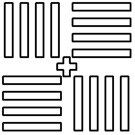
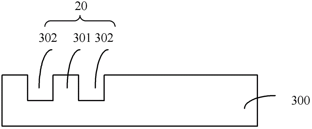
[0031] Existing super junction metal oxide layer semiconductor field effect transistors (Supper Junction MOSFET) generally need to carry out 5~7 times of epitaxial silicon layer growth process, photolithography process, and implantation process to form P-type and N-type doped regions, the inventors found During the alignment of the lithography process after the first silicon epitaxial layer process, the zero-layer mark step and shape received by the alignment sensor are relatively clear, and the alignment time has little influence on the alignment accuracy of the lithography, but in the second silicon epitaxial layer process During the alignment of the epitaxial layer growth process, especially the photolithography process after the 3rd to 7th silicon epitaxial layer growth process, the step and shape of the zero-layer mark received by the alignment sensor become less and less clear, and even deformed, which greatly It affects the accuracy of the alignment, resulting in the shi...


PUM

PropertyMeasurementUnit
thicknessaaaaaaaaaa

Abstract

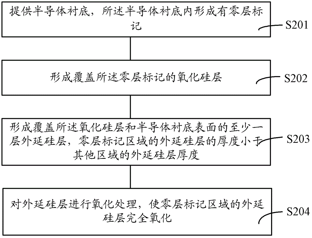
The invention provides a manufacture method of an alignment mark protective layer. The manufacture method of the alignment mark protective layer includes the following steps: providing a semiconductor substrate in which a zero-layer mark is formed, forming a monox layer which covers the zero-layer mark, forming at least one layer of epitaxial silicon which covers the monox layer and the semiconductor substrate, wherein the epitaxial silicon layer of the zero-layer mark area is thinner than the epitaxial silicon layer of the other areas, and oxygenizing the epitaxial silicon layer until the epitaxial silicon layer of the zero-layer mark area is oxygenized completely. The manufacture method of the alignment mark protective layer improves alignment precision and alignment capacity of photoetching.

Description

technical field [0001] The invention relates to the field of semiconductor manufacturing, in particular to a method for manufacturing an alignment mark protection layer in an epitaxial silicon process. Background technique [0002] The photolithography process is a key process in the manufacture of semiconductor integrated circuits, which is used to transfer the pattern on the mask plate to the surface of the wafer. However, with the continuous reduction of the feature size and the continuous improvement of the integration level of semiconductor devices, the requirements for the precision of the photolithography process are also increased. In the semiconductor manufacturing process, in order to accurately transfer the pattern on the mask to the wafer surface, the wafer must be aligned before each exposure of the photoresist. [0003] In most current epitaxial processes, the steps of using alignment marks to perform photolithographic alignment include: providing a semiconduc...

Claims


Application Information

Patent Timeline
Patent Type & Authority Patents(China)
IPC IPC(8): H01L21/02G03F9/00H01L23/544
Inventor 王刚宁唐凌李远哲朱立平梁国亮
Owner SEMICON MFG INT (SHANGHAI) CORP
Learn More