High-gain level switching circuit

A conversion circuit, high-gain technology, applied in the field of level conversion stage improvement, can solve problems such as phase delay

Inactive Publication Date: 2013-04-24
苏州硅智源微电子有限公司
View PDF6 Cites 3 Cited by
  • Summary
  • Abstract
  • Description
  • Claims
  • Application Information

AI Technical Summary

Problems solved by technology

On the downside, the differential operation of the PNP transistor and the current mirror can cause significant phase delay on high-frequency signals, similar to the level shifting stage of the LM118

Method used


Image

  • High-gain level switching circuit
  • High-gain level switching circuit
  • High-gain level switching circuit

Examples


Embodiment Construction

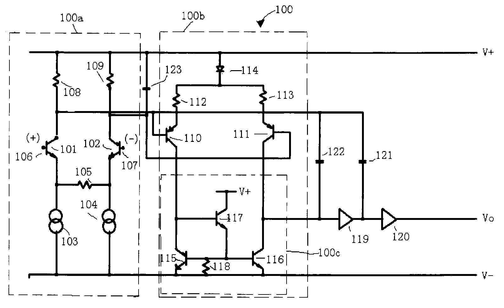
[0026] figure 1 Shown is a simplified universal operational amplifier 100, including a differential input stage 100a and a level conversion stage 100b, transistors 101 and 102, current sources 103 and 104, and resistors 105, 108 and 109 from the differential input stage 100a . The differential input voltage is suitable for generating an amplified differential voltage between the non-inverting input terminal 106 and the inverting input terminal 107 of the amplifier 100 to appear between the collectors of the transistors 101 and 102. The voltage is applied to the bases of the PNP transistors 110 and 111 at the level conversion stage 100b, and is converted into a differential current on the collectors of the PNP transistors 110 and 111. The quiescent current to the PNP transistors 110 and 111 is determined by the resistance of the resistors 112 and 113. The differential current flows into the current mirror 100c, including transistors 115 and 116, which convert the differential c...


PUM


Abstract

A high-gain level switching circuit does not restrain the upper limit of the common-mode input range of an operational amplifier. When the operational amplifier operates at specified low supply voltage, the upper limit of the common-mode input range is very important. Important parameters such as gain and switching speed of the operational amplifier can be controlled in the condition of no affecting the common-mode input voltage range. The high-gain level switching circuit works in a non-differential mode so that the problem of stability of a difference circuit is solved. The high-gain level switching circuit has the advantage of improving the gain through current balancing.

Description

Technical field [0001] The invention relates to the improvement of the performance of an integrated circuit amplifier. More particularly, the present invention relates to the improvement of the level conversion stage of an amplifier. Background technique [0002] In a typical voltage amplifier, several NPN common emitters are usually connected in series to obtain a high voltage gain. In discrete amplifiers, large capacitors can be used to combine the AC signal from one gain stage with the next level that does not affect the DC bias in the amplifier. However, in integrated amplifiers, large capacitors are usually not available because they require a large amount of chip area. Therefore, in order to ensure sufficient low frequency response, the gain stage of the integrated amplifier is usually DC coupled. However, the output DC level of an NPN common emitter gain stage is higher than its input DC level. Therefore, in a cascade of such gain stages, the DC level increases, and it...

Claims


Application Information

Patent Timeline
IPC IPC(8): H03F3/45H03F19/00
Inventor 包兴坤
Owner 苏州硅智源微电子有限公司
Why Eureka
Try Eureka