Chip provided with multiplex pin

A technology of multiplexing pins and chips, applied in the direction of logic circuit connection/interface layout, etc., can solve the problems of increasing package size, high packaging cost, unfavorable miniaturization design, etc., and achieve the goal of reducing pins and packaging area Effect

Active Publication Date: 2013-04-24
WUXI ZGMICRO ELECTRONICS CO LTD
View PDF4 Cites 20 Cited by
  • Summary
  • Abstract
  • Description
  • Claims
  • Application Information

AI Technical Summary

Problems solved by technology

[0004] But for the case where the package pins are tight, increasing the pins will increase the package size, which will increase the size o

Method used


Image

  • Chip provided with multiplex pin
  • Chip provided with multiplex pin
  • Chip provided with multiplex pin

Examples


Embodiment Construction

[0023] In order to make the above objectives, features and advantages of the present invention more obvious and understandable, the present invention will be further described in detail below with reference to the accompanying drawings and specific embodiments.

[0024] The "one embodiment" or "embodiment" referred to herein refers to a specific feature, structure, or characteristic that can be included in at least one implementation of the present invention. The appearances of "in one embodiment" in different places in this specification do not all refer to the same embodiment, nor are they separate or selectively mutually exclusive embodiments with other embodiments. Unless otherwise specified, the words connected, connected, and connected in this text indicating electrical connection all mean direct or indirect electrical connection.

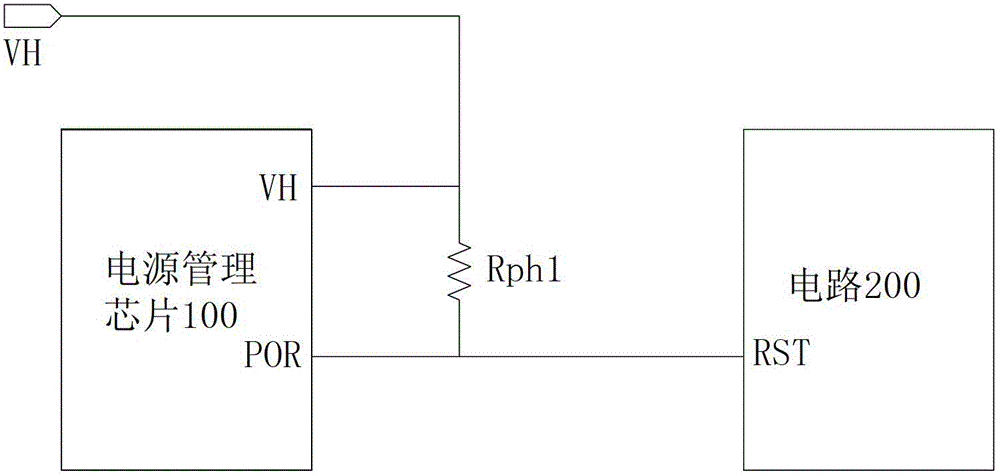
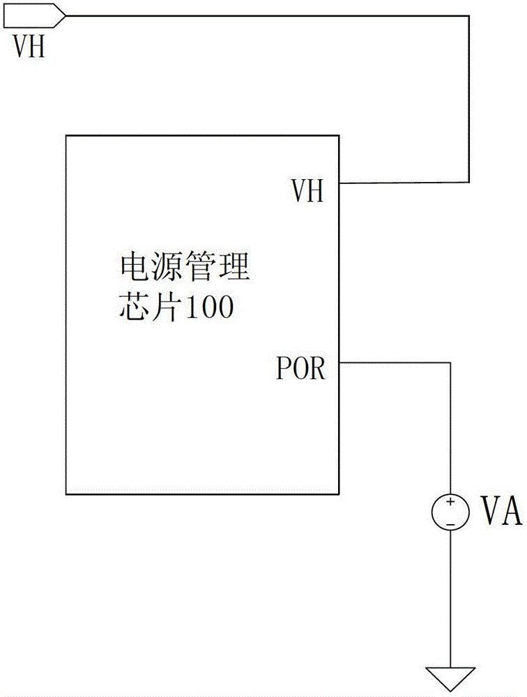
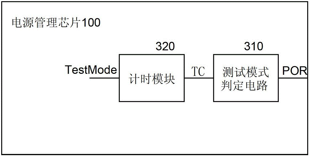
[0025] In the present invention, the test pin is multiplexed with another pin, so that the power management chip has a test mode without adding c...


PUM


Abstract

The invention provides a chip provided with a multiplex pin. The chip comprises the multiplex pin. When the multiplex pin is applied to another pin besides a test pin, voltage of the multiplex pin is larger than first threshold voltage or smaller than second threshold voltage. When the voltage of the multiplex pin is smaller than the first threshold voltage and larger than the second threshold voltage, the chip is in a test mode, and at the moment, the multiplex pin serves as the test pin and the first threshold voltage is larger than the second threshold voltage. Compared with the prior art, the chip is provided with the multiplex pin, whether the multiplex pin serves as the test pin is confirmed through testing of the voltage of the multiplex pin. The multiplex pin can serve as other pins, so the number of pins of the chip is reduced and a packaging area is reduced.

Description

【Technical Field】 [0001] The invention relates to the field of circuit design, in particular to a chip with multiplexed pins. 【Background technique】 [0002] In the prior art, a power management chip (or integrated circuit) usually uses an independent pin (or pin PIN) to set the test mode. When the pin is connected to the power supply, the power management chip enters the test mode; when the pin is grounded, the power management chip enters the normal operating mode. [0003] Generally, the test mode is of great significance to the power management chip. For example, when the chip detects the test mode, the long delay time in some normal functions can be shortened (for example, the delay of a certain function in normal working mode is as long as 2 seconds, which is too long for the chip test time and the cost is unacceptable. For example, it can be shortened to 1 millisecond), so as to quickly verify whether its function is correct, thereby reducing the test time and the test cos...

Claims


Application Information

Patent Timeline
IPC IPC(8): H03K19/0175
Inventor 王钊尹航田文博李展
Owner WUXI ZGMICRO ELECTRONICS CO LTD
Why Eureka
Try Eureka