Large dynamic medium-high frequency analog signal digitization conversion circuit

A high-frequency analog and conversion circuit technology, applied in the direction of physical parameter compensation/prevention, etc., can solve the problems of reducing small signal processing capability, increasing chip power consumption, increasing chip noise, etc., to improve quantization resolution, expand processing range, Effects of spurious signals and noise floor reduction

Inactive Publication Date: 2013-04-24
NO 34 RES INST OF CHINA ELECTRONICS TECH GRP
View PDF5 Cites 7 Cited by
  • Summary
  • Abstract
  • Description
  • Claims
  • Application Information

AI Technical Summary

Problems solved by technology

In the electronic interference environment or technical detection application occasions, the range of the amplitude of these signals is very large. At present, the amplitude difference between the large and small signals received by the best front-end antenna can reach 120dB (about 100,0000 times), and the best high-speed The analog-to-digital conversion chip can only achieve 16-bit quantization resolution. The typical value of the digital conversion dynamic range is about 95dB, which is equivalent to about 56,000 times the amplitude difference between large and small signals. Using existing chips to simply perform digital conversion processing of large dynamic signals will lose The dynamic range above 25dB is equivalent to the signal range being compressed by almost 18 times, so the existing medium and high frequency digital conversion technology cannot meet the dynamic range conversion requirements of such signals, and many original signals will be ignored during the conversion process
[0005] In addition, from the analysis of the design and manufacture of high-speed analog-to-digital conversion chips, since the analog-to-digital conversion of medium and high-frequency analog signals must adopt parallel digital technology (serial digital technology is only suitable for low-frequency signals), the high-speed comparison integrated in the conversion chip The number of devices is about 2 N (N is the number of quantization digits), every time the number of quantization digits increases, the number of high-speed comparators that need to be integrated must double, and the increase in the number of comparators will cause a sharp increase in the state reversal current of the gate circuit, resulting in The power consumption of the chip rises rapidly, and the increase of the flip current will cause new electromagnetic interference inside the chip, which will increase the background noise of the chip output, thereby reducing the processing ability of small signals
Therefore, after the number of quantization bits of medium and high frequency analog-to-digital conversion chips has gradually increased from 8 bits to 16 bits, no matter in terms of technology, cost or use analysis, there is no further impetus for further advancement in the commercial field.

Method used


Image

  • Large dynamic medium-high frequency analog signal digitization conversion circuit
  • Large dynamic medium-high frequency analog signal digitization conversion circuit
  • Large dynamic medium-high frequency analog signal digitization conversion circuit

Examples


Embodiment Construction

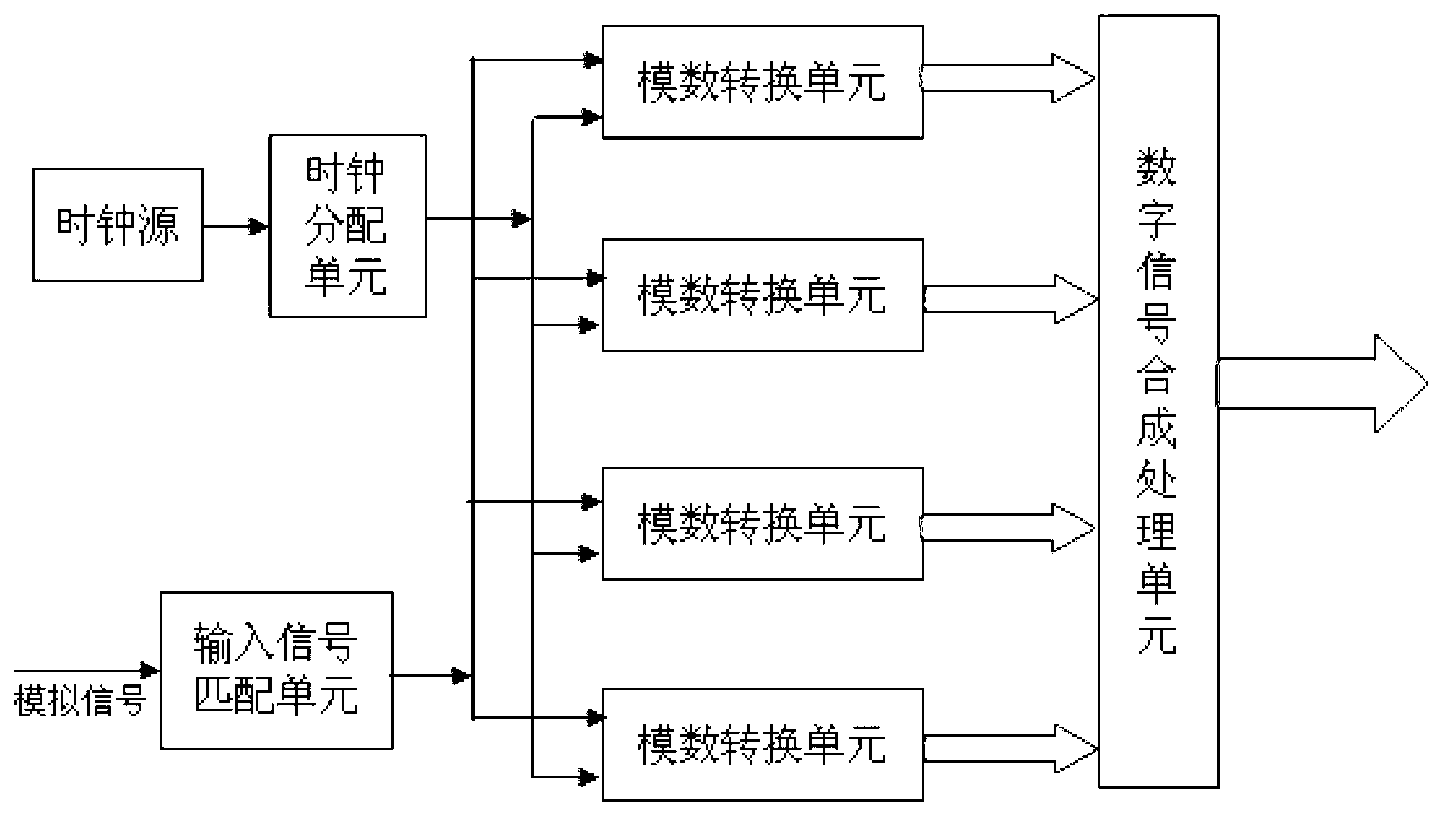
[0025] The schematic block diagram of the circuit design of this embodiment of the large dynamic medium and high frequency analog signal digitization conversion circuit is as follows: figure 1 as shown,

[0026] The clock source 6 is connected to the clock distribution unit 7. In this example, a 100MHz original frequency clock chip with low jitter and low phase noise is selected, and the spurious output spectrum is lower than -90dBm. The clock distribution unit 7 includes a clock distribution chip and its cooperating RC components. The dedicated clock processing chip in this example is a highly stable clock distribution chip with fs jitter.

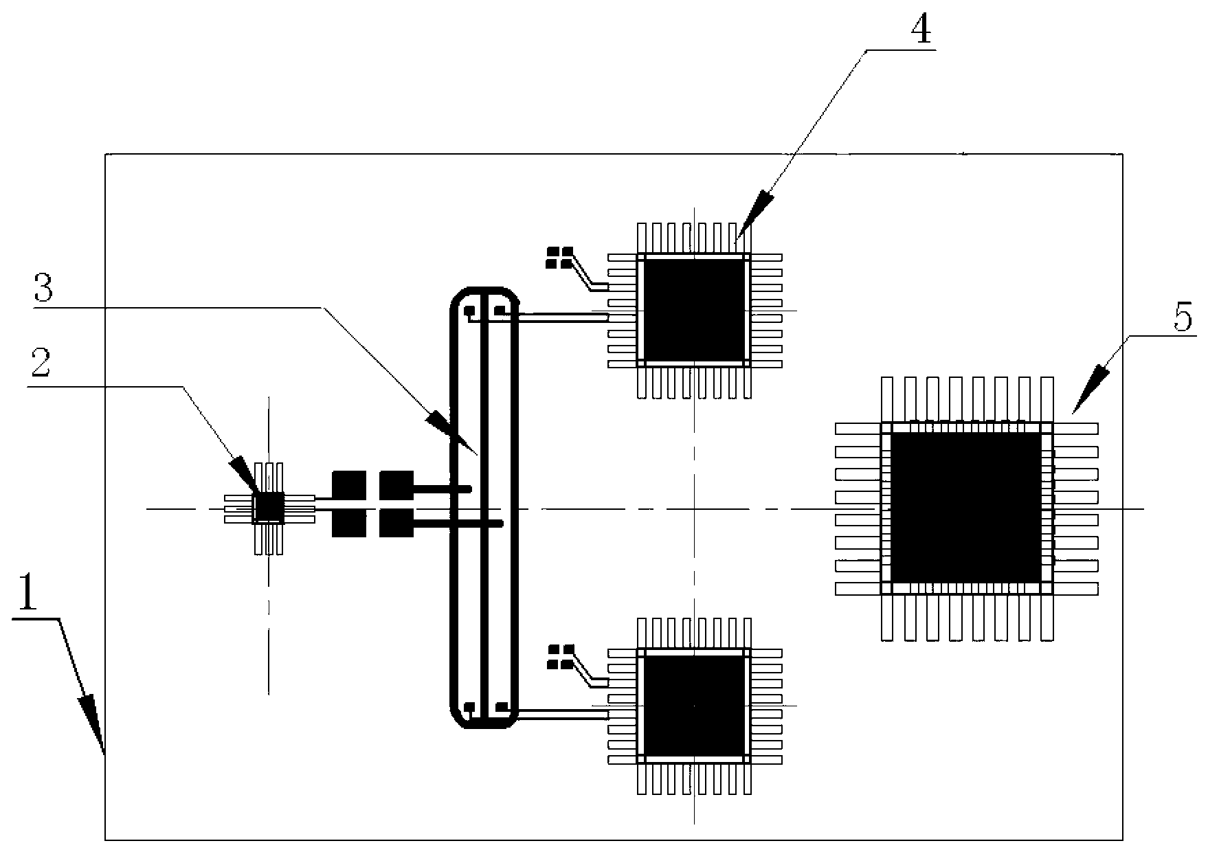
[0027] 4 identical analog-to-digital conversion units, each containing an analog-to-digital conversion chip 4, a unified external voltage reference source and its matching resistance-capacitance components, and the four analog-to-digital conversion chips 4 are the same high-speed 16-bit analog-to-digital conversion chip. In this example...


PUM


Abstract

The invention provides a large dynamic medium-high frequency analog signal digitization conversion circuit which comprises four identical analog-to-digital conversion units and a unified voltage source. Four conversion chips are identical high-speed 16-bit analog-to-digital conversion chips. Two circuit boards are arranged in a vertically and horizontally symmetrical mode. Clock signals of a clock distribution unit after being controlled and processed by a phase are accessed to the four analog-to-digital conversion chips in a difference mode. Sampling clock phases of the adjacent conversion chips differ by 180 degrees respectively. Analog difference signal lines of an input signal matching unit are accessed to the four analog-to-digital chips for parallel sampling, finish analog-to-digital conversion in a parallel mode, output 4*16-bit parallel digitization signals to a digital signal combination processing unit, and finally output high-speed digitization signals of 18-bit equivalent quantization. The four signal lines are parallel to each other and distributed in a symmetrical mode, complementary-producing magnetic field effects lower mutual electromagnetic interference degree among the chips, the number of output stray signals and noise bases is lowered, and conversion dynamic range is improved by 10-15 data bases compared with the single chip.

Description

technical field [0001] The invention relates to the technical field of remote transmission or digital acquisition of medium and high frequency analog signals, in particular to a large dynamic medium and high frequency analog signal digitization conversion circuit. Background technique [0002] The original signals in nature basically exist in the form of analog, such as sound, image, brightness, radio waves, etc. These signals must be digitized before entering the computer digital system or digital communication system, that is, analog-to-digital conversion. Convert a continuously varying analog signal into a 0 / 1 varying digitized signal. According to the frequency difference of analog signals, analog-to-digital conversion can be divided into low-frequency digital conversion technology (below 1MHz), intermediate frequency digital conversion technology (1MHz~150MHz) and high-frequency digital conversion technology (above 150MHz). If the conversion error is low, the conversio...

Claims


Application Information

Patent Timeline
Patent Type & Authority Applications(China)
IPC IPC(8): H03M1/08
Inventor 何翠平朱少林熊先越曹伟军覃桂隽王绍雷马志超
Owner NO 34 RES INST OF CHINA ELECTRONICS TECH GRP
Why Eureka
Try Eureka