Al alloy film, wiring structure having Al alloy film, and sputtering target used in producing Al alloy film
A wiring structure, sputtering target technology, applied in sputtering plating, metal/alloy conductor, semiconductor/solid-state device manufacturing, etc., can solve the problems of Al alloy corrosion, low screen display quality, etc., and achieve excellent heat resistance Effect
- Summary
- Abstract
- Description
- Claims
- Application Information
AI Technical Summary
Problems solved by technology
Method used
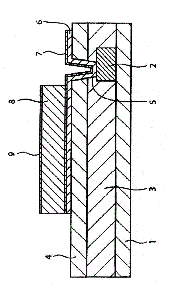
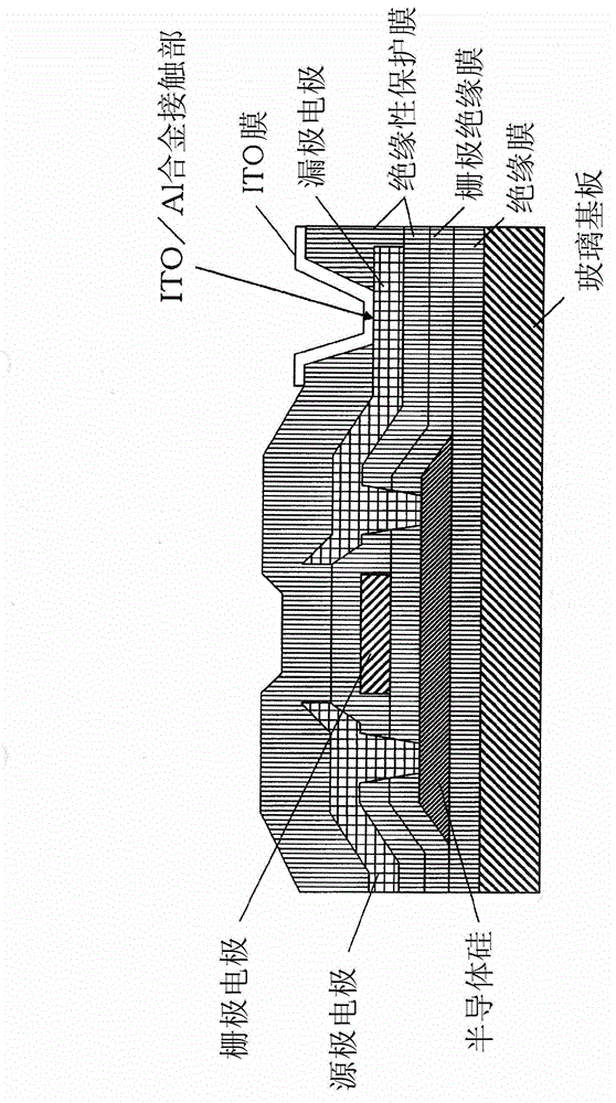
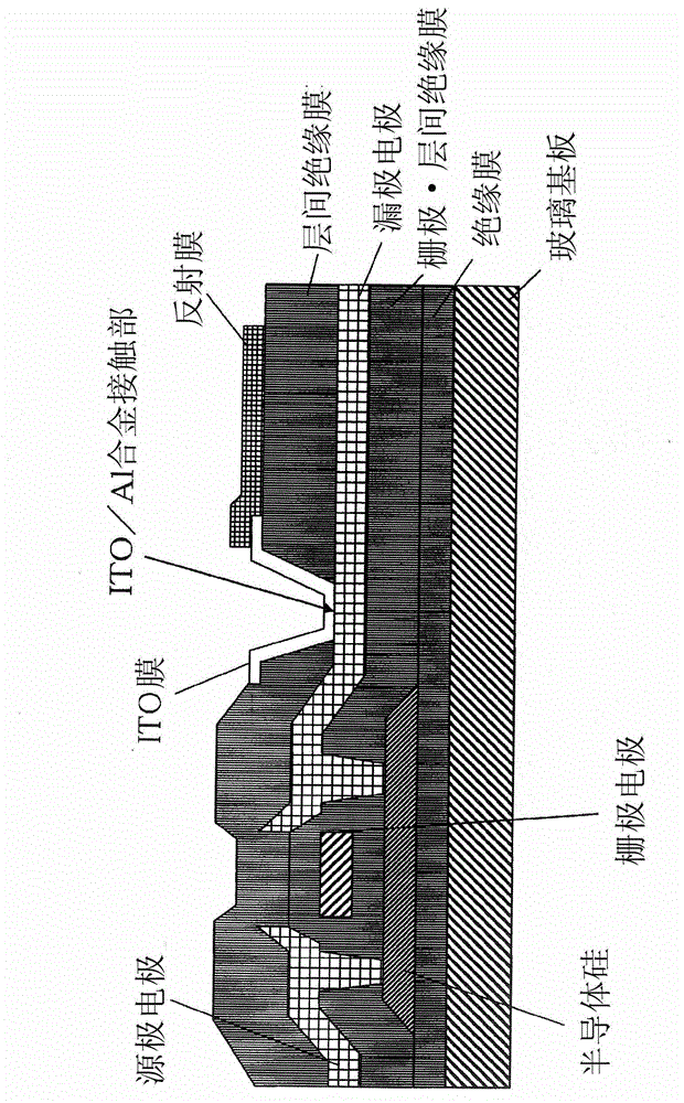
Image

Examples
Embodiment 1
[0083] In this embodiment, the following four types of samples in total were used as samples for corrosion evaluation, that is, samples (single-layer samples) in which an Al film was formed on a substrate; A sample of an ITO film (Al-ITO laminated sample); a sample in which an Al film, a high-melting-point metal film (Mo film or Ti film) and an ITO film are sequentially formed on a substrate from the substrate side (Al-high-melting-point metal- ITO laminated sample) to evaluate the corrosion resistance of sodium chloride solution. Moreover, heat resistance was evaluated about the Al-ITO laminated sample.
[0084] (Preparation of Al film monolayer sample)
[0085] By DC magnetron sputtering method (conditions: substrate = glass ("EagleXG" manufactured by Corning Corporation), atmospheric gas = argon, pressure = 2mTorr, substrate temperature = 25°C, target size = 4 inches, film formation power = 260W / 4 inch, film formation time = 100 seconds) to form Al films (film thickness ...
Embodiment 2
[0111] In this example, the Al films shown in Nos. 1 to 33 of Table 1 used in the above-mentioned Example 1 were used to produce: (iii) laminated samples: ITO films were sequentially formed on the substrate from the substrate side ( Bottom) and Al film (top) laminated sample (ITO-Al laminated sample); (iv) laminated sample: ITO film (bottom) and refractory metal film ( In the middle, a laminated sample of Mo film or Ti film) and Al film (top) (a laminated sample of ITO-refractory metal-Al); a laminated sample of (v): ITO is formed on the substrate in order from the substrate side Film (bottom), Al film (middle) and high-melting-point metal film (upper, Mo film or Ti film) laminated sample (ITO-Al-high-melting-point metal laminated sample), evaluated in the same manner as in Example 1 Corrosion resistance of sodium chloride solution.
[0112] Specifically, an ITO film (film thickness: 200 nm) was formed under the following conditions. That is, using a 4-inch ITO target, by DC...
Embodiment 3
[0126] In this example, using the Al films shown in Nos. 1 to 33 of Table 1 used in the above-mentioned Example 1, a laminated sample (Al-ITO) in which an Al film and an ITO film were sequentially formed on a substrate was produced. The ITO pinhole corrosion resistance (ITO pinhole corrosion density reduction effect) was investigated.
[0127] Specifically, by the DC magnetron sputtering method (conditions: substrate = glass ("EagleXG" of Corning Co., Ltd.), atmospheric gas = argon, pressure = 2mTorr, substrate temperature = 25 ° C, target size = 4 inches, the formation Film power = 260 W / 4 inches, film formation time = 100 seconds) formed an Al film (film thickness = 300 nm, balance: Al and unavoidable impurities) of the composition shown in Table 3 below.
[0128]In addition, the content of each element in the said Al film was calculated|required by the ICP emission analysis (induced coupling plasma emission analysis) method.
[0129] Then, heat treatment at 270° C. for 30 ...
PUM
| Property | Measurement | Unit |
|---|---|---|
| thickness | aaaaa | aaaaa |
| thickness | aaaaa | aaaaa |
| thickness | aaaaa | aaaaa |
Abstract
Description
Claims
Application Information
 - R&D Engineer
- R&D Manager
- IP Professional
- Industry Leading Data Capabilities
- Powerful AI technology
- Patent DNA Extraction
Browse by: Latest US Patents, China's latest patents, Technical Efficacy Thesaurus, Application Domain, Technology Topic.
© 2024 PatSnap. All rights reserved.Legal|Privacy policy|Modern Slavery Act Transparency Statement|Sitemap