Forming method of metal inter-lamination dielectric layer and metal inter-lamination dielectric layer

A metal layer and dielectric technology, applied in the field of inter-metal dielectric structure, can solve the problems of many steps, increased cost, reliability of metal bridges, etc.

Active Publication Date: 2013-05-08
CSMC TECH FAB2 CO LTD
View PDF7 Cites 2 Cited by
  • Summary
  • Abstract
  • Description
  • Claims
  • Application Information

AI Technical Summary

Problems solved by technology

For the first process, the filling aspect ratio (ie figure 1 In the structure where h / w) is greater than 2, obvious voids are prone to appear, so that in the subsequent manufacturing process of VIA to Metal, it is easy to cause tungsten plugs to enter the voids, resulting in metal bridges (metal bridge) or cause other reliability issues
[0007] In the second process, since fluorine-doped silica glass is deposited, a layer of orthosilicate needs to be covered to prevent the fluorine from diffusing out and crystallizing to form bubbles, which leads to more steps in the process and increases the cost and reduced productivity

Method used


Image

  • Forming method of metal inter-lamination dielectric layer and metal inter-lamination dielectric layer
  • Forming method of metal inter-lamination dielectric layer and metal inter-lamination dielectric layer
  • Forming method of metal inter-lamination dielectric layer and metal inter-lamination dielectric layer

Examples


Embodiment Construction

[0022] In order to make the objects, features and advantages of the present invention more comprehensible, specific implementations of the present invention will be described in detail below in conjunction with the accompanying drawings.

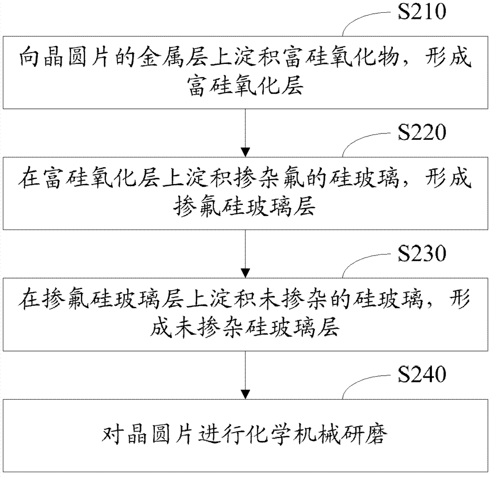
[0023] figure 2 It is a flowchart of a method for forming an inter-metal dielectric in an embodiment, including the following steps:

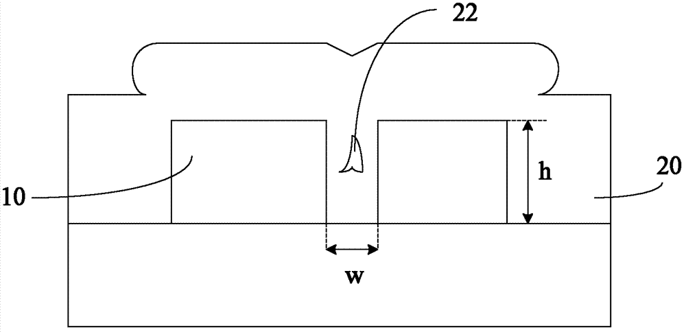
[0024] S210, depositing silicon rich oxide (Silicon Rich Oxide, SRO) on the metal layer of the wafer to form a silicon rich oxide layer. The metal layer may be the first layer M1 (ie, the metal layer covering the interlayer dielectric ILD), or any other metal layer (ie, the metal layer covering the intermetal dielectric IMD). It should be pointed out that the silicon-rich oxide layer not only covers the metal layer, but also covers the dielectric layer below the metal layer which is not covered by the metal layer. The dielectric layer is ILD (Inter layer Dielectric) for the first metal layer M1, and IMD fo...


PUM


Abstract

The invention relates to a forming method of a metal inter-lamination dielectric layer and further relates to the metal inter-lamination dielectric layer. The forming method of the metal inter-lamination dielectric layer comprises the following steps: step A, a silicon rich oxide is deposited on a metal layer of a wafer to form a silicon rich oxidation layer; step B, silicon glass with fluoride doped is deposited on the silicon rich oxidation layer to form a fluoride-doped silicon glass layer; step C, silicon glass which is of non-fluoride-doped is deposited on the fluoride-doped silicon glass layer to form a non- fluoride-doped silicon glass layer; and step D, the non-fluoride-doped silicon glass layer is formed by one side of the non-doped silicon glass layer and chemical mechanical lapping is conducted on the one side of the non-doped silicon glass layer. The fluoride-doped silicon glass is filled on the bottom of IMD (Inter-metal dielectric) and is good in filling performance, and meanwhile, non- fluoride-doped silicon glass is used as a blocking layer of the fluoride-doped silicon glass layer to prevent the fluoride from spreading. Filling quality is guaranteed, and meanwhile, required processes are less, cost is saved, and work efficiency is improved.

Description

【Technical field】 [0001] The invention relates to the field of semiconductor manufacturing, in particular to a method for forming a metal interlayer dielectric, and also to a metal interlayer dielectric structure. 【Background technique】 [0002] With the development of integrated circuit technology, the size of integrated circuits is also continuously reduced according to Moore's law, which requires continuous new technology to support the ever-increasing product requirements, especially for the requirements of the back-end process line width. is strict. For the deposition and manufacture of the existing inter-metal dielectric (IMD), the aluminum (AL) process technology can no longer fill structures with large aspect ratios, and the film stack structure currently used in the industry can no longer Meet product requirements. [0003] In the industry's traditional back-end process of aluminum wires, the following two processes are generally used for filling structures with l...

Claims


Application Information

Patent Timeline
Patent Type & Authority Applications(China)
IPC IPC(8): H01L21/768H01L23/522
Inventor 陈美丽王乐
Owner CSMC TECH FAB2 CO LTD
Why Eureka
Try Eureka