

Schottky diode and manufacturing method thereof
A technology of Schottky diodes and manufacturing methods, applied in semiconductor/solid-state device manufacturing, semiconductor devices, electrical components, etc., can solve the problems of easy breakdown of Schottky diodes and high conduction voltage, and reduce recovery time and parasitic Capacitance, reduced forward voltage, and improved high-frequency characteristics
- Summary
- Abstract
- Description
- Claims
- Application Information
AI Technical Summary
Problems solved by technology
Method used
Image


Examples
Embodiment 1
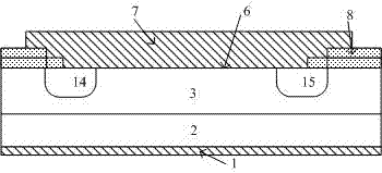
[0043] figure 2 It is a schematic diagram of the structure of the Schottky diode of the embodiment of the present invention. It can be seen from the figure that the Schottky diode of this embodiment includes N-the first semiconductor layer 3, the first metal electrode 1 formed on the back of the first semiconductor layer 3, and the metal The electrode is preferably a Ti / Ni / Ag multilayer metal, and the electrode 1 is used as the negative electrode of the Schottky diode, and is formed in the first trench 4 and the second trench 5 separated from each other in the first semiconductor layer 3, and the depth of the trench is It is preferably 2um to 7um, and the depth of the groove in this embodiment is 3um; the width of the groove is preferably 5um to 30um, and the width of the groove in this implementation is 30um, and the corners of the groove are arranged in an arc shape, which is beneficial to improve the reverse impact. breakdown voltage, the insulating layer 10 and the fillin...
Embodiment 2
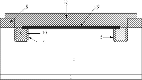
[0045] image 3It is a schematic diagram of the structure of the Schottky diode of the embodiment of the present invention. It can be seen from the figure that the Schottky diode of this embodiment includes, N+ second semiconductor layer 2, the first metal electrode 1 formed on the back of the second semiconductor layer 2, and the metal electrode It is preferably Ti / Ni / Ag, and the electrode 1 is used as the negative electrode of the Schottky diode, formed on the first semiconductor layer 3 above the second semiconductor layer, and formed in the first grooves 4 separated from each other in the first semiconductor layer 3 And the second groove 5, the depth of the groove is preferably 2um to 7um, and the present embodiment is 3um; the width of the groove is preferably 5um to 30um, and the groove width of this embodiment is 30um, and the corners of the groove are arranged as arcs shape, which is beneficial to improve the reverse breakdown voltage, the insulating layer 10 and the f...
Embodiment 3
[0047] The manufacturing method of embodiment one Schottky diode of the present invention comprises the following steps:
[0048] Step one, such as Figure 4 As shown, an N-semiconductor first semiconductor layer 3 is selected, and an oxide layer 8 is formed on the first semiconductor layer 3. The oxide layer 8 is silicon dioxide, and its thickness is preferably 200nm to 500nm. In this embodiment, 300nm is selected.
[0049] Step two, such as Figure 5 As shown, a photoresist layer 11 is formed on the oxide layer 8 .
[0050] Step three, such as Image 6 As shown, the trench window is defined, and the first trench 4 and the second trench 5 separated from each other are formed in the first semiconductor layer 3. In this embodiment, plasma etching or reactive ion etching is used in the defined window Etch to form a groove, the depth of the groove is preferably 2um to 7um, and this embodiment is 3um; the width of the groove is preferably 5um to 30um, the groove width of this e...
PUM
 Abstract
Description
Claims
Application Information