
Electroluminescence device and preparation method thereof

An electroluminescent device and electroluminescent layer technology, which is applied in the manufacture of semiconductor/solid-state devices, electric solid-state devices, electrical components, etc., can solve the problem of low light extraction efficiency and external quantum efficiency, short service life, and low device luminous efficiency. and other problems, to achieve the effect of improving light extraction efficiency, reducing power consumption and improving light efficiency

Active Publication Date: 2013-05-08
HEFEI BOE OPTOELECTRONIC TECH CO LTD +1
View PDF7 Cites 13 Cited by
  • Summary
  • Abstract
  • Description
  • Claims
  • Application Information

AI Technical Summary

Problems solved by technology

[0003] However, limited by the total reflection of the glass substrate (about 30%) and the lateral guided wave of the organic layer (about 50%), only about 20% of the photons can exit the OLED device, and the maximum external quantum efficiency of the device can only reach 17%.
The light extraction efficiency and external quantum efficiency are low, resulting in low light efficiency of the device, high power consumption, chip heating, and short service life.

Method used


Image

  • Electroluminescence device and preparation method thereof
  • Electroluminescence device and preparation method thereof
  • Electroluminescence device and preparation method thereof

Examples


Embodiment 1

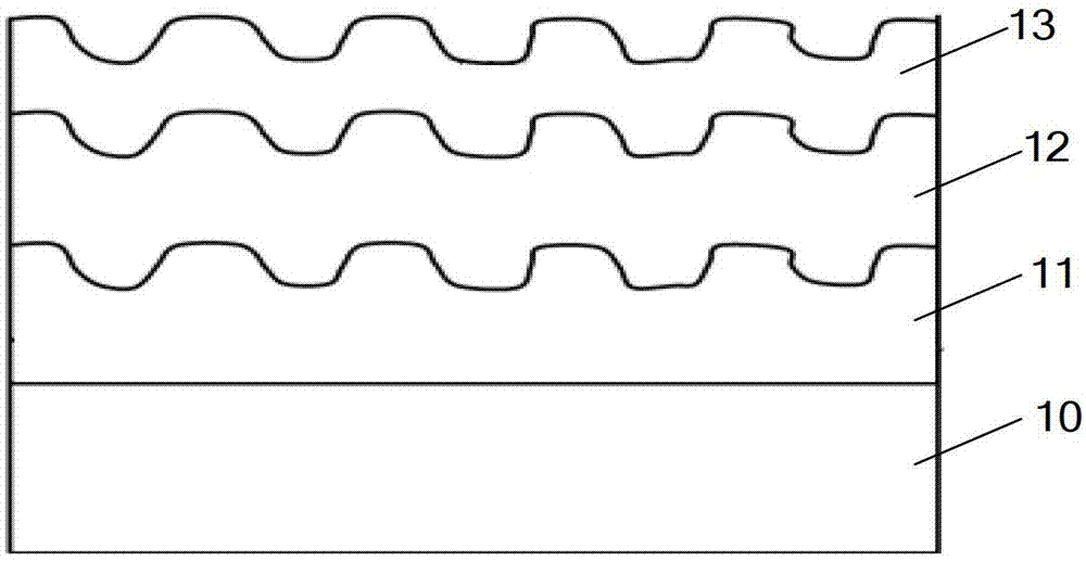
[0049] The embodiment of the present invention provides an electroluminescent device, such as figure 1 As shown, the device includes: a substrate 10; a first electrode 11 and a second electrode 13 arranged on the substrate 10, and an electroluminescent layer 12 sandwiched between the first electrode 11 and the second electrode 13; At least one of the first electrode and the second electrode is a grating structure, and the grating period of the grating structure is the first period value.

[0050] In this embodiment, if the first electrode 12 is an anode, the second electrode 13 is a cathode; if the first electrode 12 is a cathode, the second electrode 13 is an anode.

[0051] In electroluminescent devices, due to the high refractive index of the electroluminescent materials and electrode metal films, the internal lateral waveguide loss of the device is large (about 50%). Therefore, in order to obtain high-efficiency organic electroluminescent devices, reduce the device The internal...

Embodiment 2

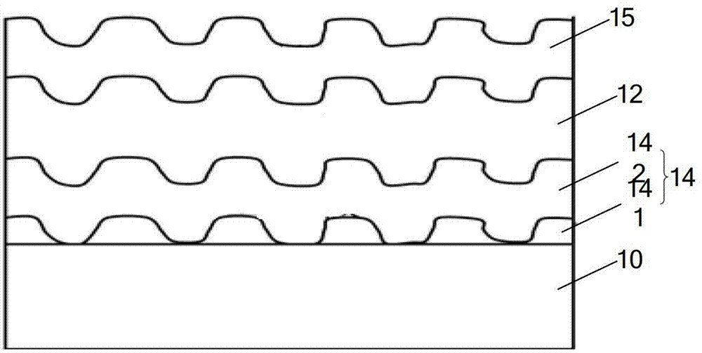
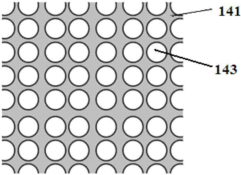
[0061] This embodiment also provides another electroluminescent device, such as figure 2 As shown, the device includes: a substrate 10; an anode 14 and a cathode 15 arranged on the substrate 10, and an electroluminescent layer 12 sandwiched between the anode 14 and the cathode 15; the light generated by the electroluminescent device is emitted from the bottom , The anode 14 is arranged in the light emission direction. The electroluminescent layer 12 includes: a first metal film layer 141 provided with a plurality of holes 143, and the holes 143 are arranged in an array in the first metal film layer 141, such as image 3 Shown; the second metal film layer 142, covering the first metal film layer 141.

[0062] The first metal film layer 141 is a hole structure distributed in an array, the second metal film layer 142 covers the first metal film layer 141, and the second metal film layer 142 corresponds to the portion of the first metal film layer 141 to the holes Protruding and for...

Embodiment 3

[0072] An embodiment of the present invention also provides an electroluminescence display device, which includes any electroluminescence device in the above-mentioned embodiments. The display device may be any product or component with display function, such as electronic paper, OLED panel, mobile phone, tablet computer, television, display, notebook computer, digital photo frame, navigator, etc. The display device adopts the electroluminescent device with high transmittance of the present invention, and thus has the advantages of high brightness, energy saving and power saving.


PUM


Abstract

The invention discloses an electroluminescence device and an electroluminescence display device, and belongs to the display field. Total reflection and waveguide effect of light in an organic layer and an anode interface can be reduced, the number of emergent photon is increased, light-taking-out efficiency of the device is improved, and therefore lighting effect is improved and power consumption is reduced. The electroluminescence device comprises a substrate, a first electrode, a second electrode, electroluminescence layer and a grating structure, wherein the first electrode and the second electrode are arranged on the substrate, the electroluminescence layer is arranged between the first electrode and the second electrode in a clamping mode, the first electrode close to the substrate is designed to be the grating structure.

Description

Technical field [0001] The invention relates to the field of display, in particular to an electroluminescent device and a manufacturing method thereof. Background technique [0002] Organic Light Emitting Diode (OLED) display has self-luminescence at the same time, no backlight, high contrast, thin thickness, wide viewing angle, fast response speed, can be used for flexible panels, wide temperature range, structure and Excellent features such as simple manufacturing process are considered to be the emerging technology of the next generation of flat panel displays. [0003] However, limited by the total reflection of the glass substrate (about 30%) and the lateral guided wave (about 50%) of the organic layer, only about 20% of the photons can be emitted from the OLED device, and the maximum external quantum efficiency of the device can only reach 17% . The low light extraction efficiency and external quantum efficiency lead to problems such as low light efficiency of the device, h...

Claims


Application Information

Patent Timeline
Patent Type & Authority Applications(China)
IPC IPC(8): H01L51/52H01L51/56
CPCH01L51/5268H10K50/854H10K50/81
Inventor 郭远辉王辉王春张一三
Owner HEFEI BOE OPTOELECTRONIC TECH CO LTD
Learn More