Processing method of printed circuit board (PCB) and PCB

A processing method and technology for PCB boards, applied in the direction of secondary processing of printed circuits, etc., can solve the problems of poor tin surface quality, affecting the quality of PCB, and the effect of removing moisture is not obvious, so as to solve the problem of board edge delamination, Improve the problem of edge delamination and improve the effect of edge delamination

Active Publication Date: 2013-05-08
GUANGDONG SHENGYI SCI TECH
View PDF5 Cites 14 Cited by
  • Summary
  • Abstract
  • Description
  • Claims
  • Application Information

AI Technical Summary

Problems solved by technology

However, in actual operation, due to the presence of copper-plated packages on the edge of the PCB, water vapor cannot escape from the edge of the PCB, and the effect of baking to remove moisture is not obvious, and the problem of delamination on the edge of the HASL cannot be improved.
[0005] In the prior art, it is often used to reduce the temperature of HASL and shorten the time of immersion tin to overcome the problem of delamination of the edge of HASL. Properly reducing the temperature of HASL and shortening the time of immersion tin can improve the edge of HASL to a certain extent. Delamination problem, but it will cause follow-up problems such as poor tin surface quality, so this method is not the best way to improve the delamination problem of HASL
[0006] Looking at the methods for improving the delamination of PCB boards in the prior art, the existing defects are: the technical means cannot improve or can not better improve the delamination of the PCB board edge in the tin spraying process, or the technical means can to a certain extent Improve the delamination problem of the tin plate, but it will cause a series of follow-up problems, which will still affect the quality of the PCB

Method used


Image

  • Processing method of printed circuit board (PCB) and PCB
  • Processing method of printed circuit board (PCB) and PCB
  • Processing method of printed circuit board (PCB) and PCB

Examples


Embodiment 1

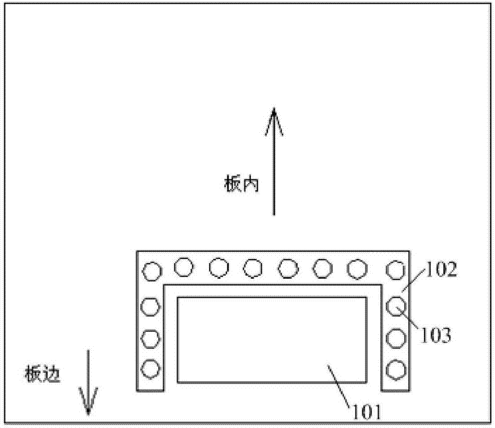
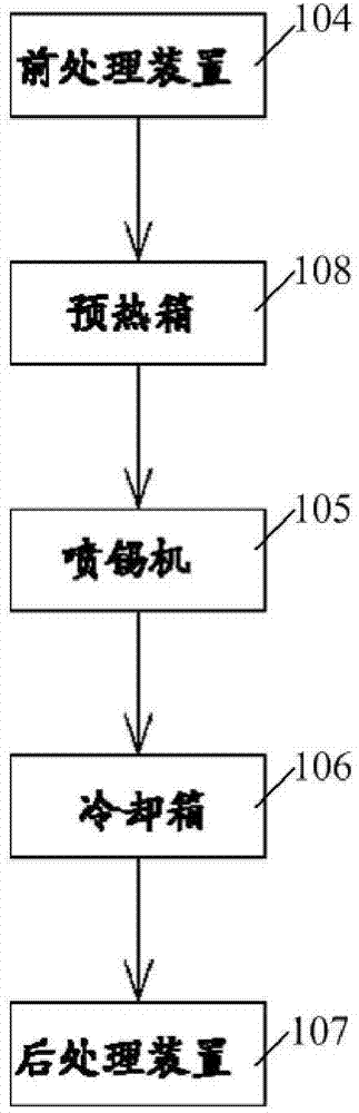
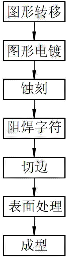
[0048] Using S1155 1.61 / 1 to make a double-sided panel with a total of 10PNL, the outer layer processing process is graphic transfer→graphic plating→etching→solder resist characters→baking→surface treatment→molding. The surface treatment process is tin spraying, and the tin spraying parameters are: temperature 260°C, tin immersion time 3s, air knife temperature 380°C. After the tin spraying is completed, inspect and evaluate the quality of the tin surface of the board; at the same time, visually inspect and analyze the edge of the PCB board to understand the delamination of the board edge.

Embodiment 2

[0050] Using S11551.61 / 1 to make a double-sided panel with a total of 10PNL, the outer layer processing process is graphic transfer→graphic plating→etching→solder resist characters→baking→surface treatment→molding. The surface treatment process is tin spraying, and the tin spraying parameters are: temperature 240°C, tin immersion time 2s, air knife temperature 340°C. The baking process before HASL is: 150℃ / 2hr. After the tin spraying is completed, inspect and evaluate the quality of the tin surface of the board; at the same time, visually inspect and analyze the edge of the PCB board to understand the delamination of the board edge.

Embodiment 3

[0052] Use S11551.61 / 1 to make a double-sided board with a total of 10PNL, such as image 3 As shown, the outer layer processing technology is graphic transfer→graphic electroplating→etching→solder resist characters→edge trimming process→surface treatment→molding. The surface treatment process is tin spraying, and the tin spraying parameters are: temperature 260°C, tin immersion time 3s, air knife temperature 380°C. After the tin spraying is completed, inspect and evaluate the quality of the tin surface of the board; at the same time, visually inspect and analyze the edge of the PCB board to understand the delamination of the board edge.


PUM


Abstract

The invention discloses a processing method of a printed circuit board (PCB) and the PCB. The processing method includes a first step of eliminating a copper layer arranged at the edge of the PCB before a step of solder coating surface treatment and a second step of heating the PCB after eliminating the copper layer arranged at the edge of the PCB. Due to the facts that the copper layer wrapping the edge of the PCB is eliminated before solder coating, base materials of PCB board sides are exposed, and moisture can be directly eliminated by the PCB board sides when the solder coating is conducted successively, a problem of board side delamination is improved. Heating is conducted after the copper layer which wrapps the edge of the PCB is eliminated, residual moisture in the PCB can be actively eliminated, and therefore the problem of board side delamination in the process of the following solder coating is fundamentally solved. The processing method of the PCB can be finished by means of PCB convention processing equipment and therefore the processing method of the PCB is easy to achieve and low in cost.

Description

technical field [0001] The invention relates to the technical field of printed circuit boards, in particular to a PCB processing method for improving PCB edge delamination and a PCB manufactured by the method. Background technique [0002] PCB (Printed Circuit Board), the Chinese name is a printed circuit board, which is a support for electronic components and provides electrical connections for electronic components. In the process of PCB board processing, the outer process flow is generally: graphic transfer→graphic plating→etching→solder resist characters→surface treatment→forming processing. Common surface treatment processes include hot air leveling (HASL, Hot Air Solder Leveling, commonly known as tin spraying) treatment, gold plating treatment, OSP (Organic Solderability Preservatives) organic solder protection film treatment, etc. Among them, the tin spraying treatment directly removes the PNL board of the PCB Extending into the high-temperature tin furnace to immer...

Claims


Application Information

Patent Timeline
Patent Type & Authority Applications(China)
IPC IPC(8): H05K3/22
Inventor 李龙飞王水娟方东炜杨涛吴小连
Owner GUANGDONG SHENGYI SCI TECH
Why Eureka
Try Eureka