Ink box chip used for printer and ink box containing ink box chip

A technology of printers and ink cartridges, which is applied in printing and other directions, can solve the problem of small chip size, achieve the effect of small chip area, save space, and reduce the probability of short circuit

Active Publication Date: 2013-05-15
APEX MICROELECTRONICS CO LTD
View PDF8 Cites 28 Cited by
  • Summary
  • Abstract
  • Description
  • Claims
  • Application Information

AI Technical Summary

Problems solved by technology

[0006] The invention provides a chip for an ink cartridge used in a printer to solve the technical problem that the existing chip for an ink cartridge used in a printer cannot simultaneously satisfy the small size of the chip and ensure good contact between the contact and the elastic contact of the printer

Method used


Image

  • Ink box chip used for printer and ink box containing ink box chip
  • Ink box chip used for printer and ink box containing ink box chip
  • Ink box chip used for printer and ink box containing ink box chip

Examples


Embodiment 1

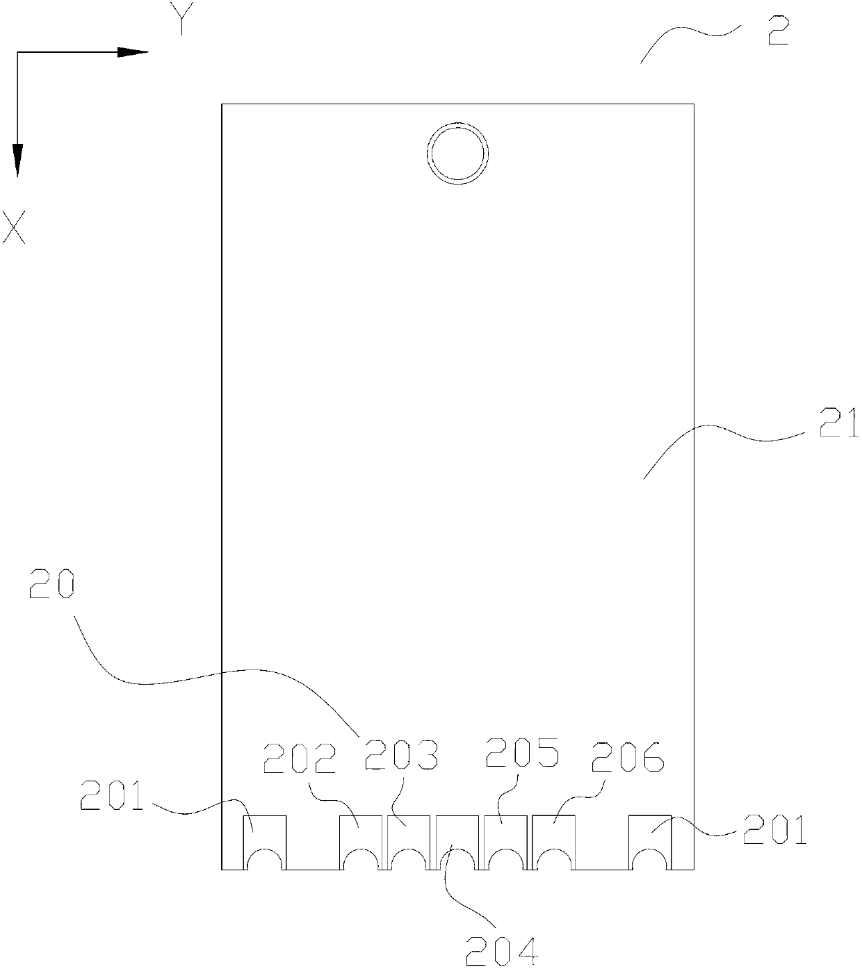
[0030] A chip used in ink cartridges used in printers, such as image 3 As shown, the chip 2 includes a substrate 21, a device circuit (not shown in the figure) and a plurality of contact terminals 20, and the plurality of contact terminals 20 include two high-voltage terminals 201, a power supply terminal 202, a clock terminal 203, and a ground terminal 204 , reset terminal 205 and data terminal 206; the high-voltage terminal 201 is arranged at both ends of the entire row of contacts, and the distance between the high-voltage terminal and other terminals is greater than the distance between other terminals; the ground terminal 204 is arranged at the two ends of the entire row of contacts In the middle, the ground terminal is farther from the high voltage terminal than any of the other contact terminals.

[0031] At least a part of each contact terminal in the plurality of contact terminals 20 is arranged on a straight line, at least one contact terminal in the plurality of co...

Embodiment 2

[0037] Figure 5 It is a schematic diagram of the chip structure of the second embodiment of the present invention, as shown in the figure, on the basis of the first embodiment, this embodiment makes the following improvements: the chip 2 includes a substrate 21, a device circuit (not shown in the figure) and a plurality of contacts Terminal 20, among the plurality of contact terminals 20, there are contact terminals 22 that only include the first contact surface, and contact terminals that include both the first contact surface and the second contact surface. Specifically, the chip in this implementation The clock terminal 220 and reset terminal 221 are contact terminals that only include the first contact surface (hereinafter referred to as the first group of contact terminals), and the rest are contact terminals that include both the first contact surface and the second contact surface ( Hereinafter referred to as the second group of contact terminals), the first group of c...

Embodiment 3

[0041] This embodiment is a modified example of Embodiment 1, such as Figure 7 As shown, the difference from Embodiment 1 is that the chip contact provided by this embodiment includes three contact surfaces, namely the first contact surface 23b located on the substrate layout surface and the third contact surface 23c perpendicular to the substrate layout surface, and the Between the first contact surface 23b and the third contact surface 23c, there is a second contact surface 23a with rounded or chamfered corners. The second contact surface 23a is a groove with an arc or slope. When the ink cartridge is installed in the printer, the elastic contacts of the printer are preferentially in contact with the second surface contact 23a. When the ink cartridge where the chip is located is caused by process errors and other problems, the depth of the chip installation is different, such as when the chip installation position is lower or higher. After the chip is loaded into the inkjet...


PUM


Abstract

The invention relates to an ink box chip used for a printer. The ink box chip used for the printer comprises a base plate, a device circuit arranged on the base plate and multiple contact terminals. The multiple contact terminals comprises a power supply terminal, a ground terminal, a reset terminal, a clock terminal, a data terminal and high-pressure terminals, wherein the high-pressure terminals are inflicted a high voltage by the printer, the high-pressure terminals are arranged at two ends of the whole row contact terminals. At least one contact terminal among the multiple contact terminals comprises a first contact surface and a second contact surface, wherein the first contact surface is arranged on an arrangement surface on the base plate, and the arrangement surface on the base plate corresponds to an elastic contact on the printer, the second contact surface is arranged on an inserting end surface on the base plate when the ink box is inserted into the printer, and a concave groove is arranged on the second contact surface. Namely, parts or all the multiple contact terminals are arranged on two adjacent surfaces. An area of the chip can be produced smaller, and space is saved. Meanwhile, the printer can still be in good contact under the conditions of the smaller chip area ensured.

Description

technical field [0001] The invention relates to the technical field of imaging and development, in particular to a chip for an ink box used in a printer and an ink box containing the chip. Background technique [0002] Inkjet printers are widely used in the office field, and their styles are becoming more and more diverse. Most of the existing inkjet printers use detachable ink cartridges, which are installed on the main body of the printer and deliver the ink to the recording medium. Ink cartridges generally have chips that store ink-related information. An existing chip includes a storage device that stores information such as the ink cartridge model, production date, and ink volume, and a high-voltage circuit that outputs a response signal based on the application of a voltage higher than the power supply voltage of the storage device (for example, used as an ink remaining The piezoelectric element of the amount sensor, or the analog circuit of the analog ink amount inf...

Claims


Application Information

Patent Timeline
Patent Type & Authority Applications(China)
IPC IPC(8): B41J2/175
Inventor 刘卫臣
Owner APEX MICROELECTRONICS CO LTD
Why Eureka
Try Eureka