Gradient AlGaN layer preparation method and device prepared by same

A technology of buffer layer and epitaxy, which is applied in semiconductor devices, semiconductor/solid-state device manufacturing, electrical components, etc., can solve the problem of inability to effectively adjust the stress and dislocation density of GaN thin films, slow growth rate, and affecting the quality of GaN thin film crystals, etc. problem, to achieve the effect of controllable distribution and high crystal quality

Active Publication Date: 2013-05-22
SUN YAT SEN UNIV
View PDF5 Cites 16 Cited by
  • Summary
  • Abstract
  • Description
  • Claims
  • Application Information

AI Technical Summary

Problems solved by technology

However, this method can only grow a graded AlGaN layer with a single aluminum composition distribution, but cannot adjust the distribution of its aluminum composition, so it cannot effectively adjust the stress and dislocation density of the GaN film, which affects the crystal quality of the GaN film.
[0007] In addition, since TMAl and NH 3 Has a strong pre-reaction, which makes it difficult to grow AlGaN with a high aluminum composition, and the growth rate is very slow
Therefore, if only the flow rates of TMAl and TMGa change linearly, the thickness of AlGaN with high aluminum composition will be

Method used


Image

  • Gradient AlGaN layer preparation method and device prepared by same
  • Gradient AlGaN layer preparation method and device prepared by same
  • Gradient AlGaN layer preparation method and device prepared by same

Examples


Embodiment 1

[0035] The method for preparing a graded AlGaN layer according to an embodiment of the present invention includes the following steps:

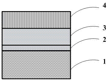
[0036] S1. growing a layer of high-temperature AlN layer 2 on the Si substrate 1 as a buffer layer;

[0037] S2. Growing a graded AlGaN layer 3 on the high-temperature AlN layer 2 .

[0038]After the graded AlGaN layer is prepared, the GaN thin film 4 and other required material layers can be grown sequentially on the graded AlGaN layer 3 to obtain the desired device.

[0039] Such as figure 1 As shown, it is a schematic diagram of the device structure obtained by epitaxially growing a GaN thin film on the graded AlGaN layer obtained by the above method, including a Si substrate 1, a high-temperature AlN layer 2, a graded AlGaN layer 3 and a GaN thin film 4 from bottom to top.

[0040] Wherein, the thickness of the graded AlGaN layer 3 is 1 μm, the growth temperature is 990° C., the growth pressure is 100 mbar, and the V / III ratio is 2000. ...

Embodiment 2

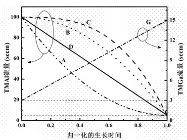
[0045] This embodiment is similar to Embodiment 1, the only difference being that the functions of the TMAl and TMGa flow rates are different from those of Embodiment 1, specifically: during the growth of the graded AlGaN layer, the TMAl flow rate drops from 100 sccm to 5 sccm, and its function is B= 100-95 x 2 (sccm), TMGa flow increases linearly from 3 sccm to 15 sccm, and its function curve is G=12 x +3 (sccm). in the above function x (0≤ x ≤1) is the normalized time for the growth of the graded AlGaN layer. Function curve such as figure 2 shown.

Embodiment 3

[0047] This embodiment is similar to Embodiment 1, the only difference being that the function of the flow of TMAl and TMGa is different from that of Embodiment 1, specifically: the flow of TMAl in the graded AlGaN layer drops from 100 sccm to 5 sccm, and its function is C=100- 95 x 3 (sccm), TMGa flow increases linearly from 3 sccm to 15 sccm, and its function curve is G=12 x +3 (sccm). In the above two functions x (0≤ x ≤1) is the normalized time for the growth of the graded AlGaN layer. Function curve such as figure 2 shown.

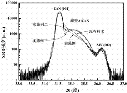
[0048] In order to better illustrate the effectiveness of a method for preparing a graded AlGaN layer of the present invention, the linear function in the prior art is used as a comparison, which is basically similar to that in the examples, except that the function of the TMAl and TMGa flow rates is the same as Different from Example 1, a linear function is adopted, specifically: during the growth process of the gradient AlGaN layer, the TM...


PUM

PropertyMeasurementUnit
Growth temperatureaaaaaaaaaa
Thicknessaaaaaaaaaa
Thickness rangeaaaaaaaaaa

Abstract

The invention relates to the technical field of semiconductors, in particular to a gradient AlGaN layer preparation method and a device prepared by the same. When a gradient AlGaN layer is grown, flow of trimethylaluminum fed into a reaction chamber is gradually decreased, and flow of trimethylgallium is increased gradually. The function of the trimethylaluminum flow satisfies yTMAl=a-bx<m> or yTMAl=a(1-x)<m>+b, the function of the trimethylgallium flow satisfies yTMGa=cx<n>+d or yTMGa=c-d(1-x)<n>, x refers to normalization time of growing of the gradient AlGaN layer, and m and n are 1 asynchronously. By the aid of the different flow functions, change rates of TMAl and TMGa in different flows are changed, so that distribution of aluminum in the gradient AlGaN layer can be controlled effectively, further stress and crystalline quality of a GaN film growing on the gradient AlGaN layer are regulated and controlled, and a thick GaN film high in crystalline quality and free of crazing is grown.

Description

technical field [0001] The invention relates to the technical field of semiconductors, and more specifically, to a preparation method of a graded AlGaN layer and a device obtained by the method. Background technique [0002] GaN has the characteristics of large direct band gap (3.4 eV), high thermal conductivity, high electron saturation drift velocity and large critical breakdown voltage, so it has become a research hotspot in the field of semiconductor technology. The band gaps of the group III nitrides GaN, AlN (band gap 6.2 eV), InN (band gap 0.7 eV) and their alloys cover the energy range from infrared to visible light and ultraviolet light, so they have great potential in the field of optoelectronics. A wide range of applications, such as high-power white LEDs, ultraviolet and blue lasers, solar-blind detectors in the ultraviolet band, high-frequency high-power devices, etc. [0003] Due to the difficulty in growing large-sized GaN single crystals, it is difficult to ...

Claims


Application Information

Patent Timeline
IPC IPC(8): H01L21/02H01L29/20
Inventor 张佰君杨亿斌
Owner SUN YAT SEN UNIV
Why Eureka
Try Eureka