Reflection-type photoetching projection objective
A lithography projection and reflection technology, applied in microlithography exposure equipment, optics, optical components, etc., can solve the problems of increased difficulty in manufacturing objective lenses, low exposure efficiency, and increased cost, and achieves high transmittance, increased Exposure illuminance, the effect of improving productivity
- Summary
- Abstract
- Description
- Claims
- Application Information
AI Technical Summary
Problems solved by technology
Method used
Image

Examples
Embodiment Construction
[0024] Specific embodiments of the present invention will be described in detail below in conjunction with the accompanying drawings.
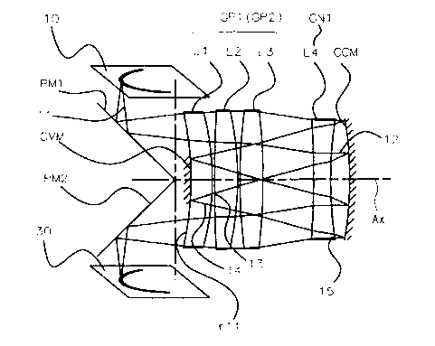
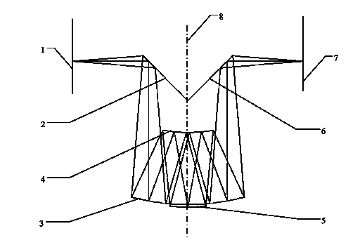
[0025] Projection objective lens optical system structure of the present invention such as figure 2 As shown, after the mask surface 1 is irradiated by illumination light, the light passing through the mask is reflected by the plane reflector 2 and then enters the spherical reflector 3. The plane reflector 2 makes the chief ray of each object point reflect at 90 degrees. The concave spherical mirror 3 has a positive power, so that the light falling on it can be partially converged and reflected. The light reflected from the spherical reflector 3 enters the spherical reflector 4, and the spherical reflector 4 has a negative power, so that the reflected light can enter the spherical reflector 5 in a divergent form. The light rays of each object point form a pupil surface on the spherical mirror 5 after passing through the above-mentioned optic...
PUM
 Abstract
Description
Claims
Application Information