
Lithography Projection Objectives

A technology of lithography projection and objective lens, which is applied in the direction of microlithography exposure equipment, optics, optical components, etc., can solve the problems of increased difficulty in objective lens manufacturing, increased cost, low exposure efficiency, etc., achieve excellent exposure image quality, improve production rate, increase the effect of exposure illumination

Active Publication Date: 2016-02-03
SHANGHAI MICRO ELECTRONICS EQUIP (GRP) CO LTD
View PDF6 Cites 0 Cited by
  • Summary
  • Abstract
  • Description
  • Claims
  • Application Information

AI Technical Summary

Problems solved by technology

[0004] 2. In order to ensure aberration, monochromatic light exposure is used, and the exposure efficiency is low;
[0005] 3. In order to improve the aberration, 2 to 4 large-diameter glass material lenses are used, which makes the manufacture of the objective lens more difficult, the cost is increased, and the weight is heavier

Method used


Image

  • Lithography Projection Objectives
  • Lithography Projection Objectives
  • Lithography Projection Objectives

Examples


Embodiment 1

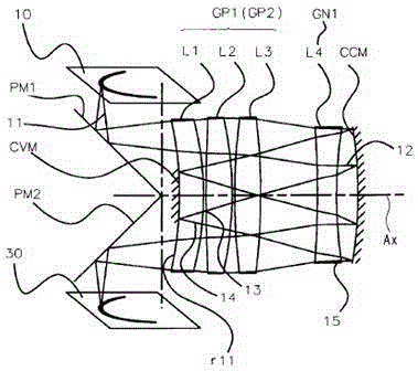
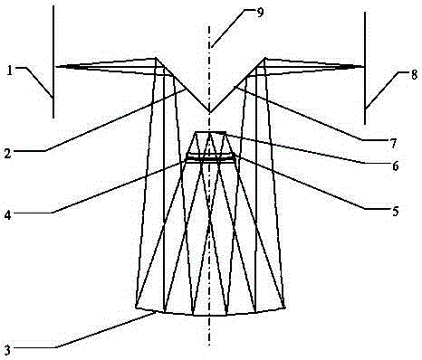
[0027] Projection objective lens optical system structure of the present invention such as figure 2 shown. After the mask surface 1 is irradiated by the illumination light, the light passing through the mask is reflected by the plane reflector 2 and then enters the spherical reflector 3. The plane reflector 2 makes the chief ray of each object point reflect at 90 degrees. The concave spherical reflector 3 has positive refractive power, so that the light falling on it can be partially converged and reflected, and the light reflected from the spherical reflector 3 enters the lens 4 and the lens 5 in turn, and the lens 4 and the lens 5 have negative power respectively. Refractive power and positive refractive power, the light rays of each object point form a pupil surface on the spherical mirror 6 after passing through the above-mentioned optical components. After the light is reflected by the spherical mirror with negative refractive power, it passes through lens 5, lens 4, an...

Embodiment 2

[0037] Embodiment 2 of the present invention is based on Embodiment 1. The spherical surfaces of the two lenses 4 and 5 are changed to aspheric surfaces to correct more different types of aberrations and obtain excellent image quality patterns in the exposure area.

[0038] The structural data of this embodiment is as follows:

[0039]

[0040]

[0041] The parameters of each aspheric surface are as follows:

[0042] Surface

[0043] In this embodiment the wave aberration RMS value is as Figure 5 As shown, the maximum is 0.0111λ, and λ takes the wavelength of the h line (404.65nm).


PUM

PropertyMeasurementUnit
diameteraaaaaaaaaa

Abstract

Provided is a photoetching projective objective glass. The photoetching projective objective glass comprises a first plane mirror, a first spherical mirror which is provided with positive light focal power, a lens group provided with negative light focal, a second spherical mirror and a second plane mirror which are provided with negative light focal power, and a second plane mirror; light successively passes through the first plane mirror, the first spherical mirror, the lens group, the second spherical mirror, the lens group, the first spherical mirror and the second plane mirror along the transmission direction. The photoetching projective objective glass has a pretty big exposure field, and a non-scanning direction is 500 millimeters; by using a multi-wavelength for exposure, exposure illumination is increased, and productivity of a photoetching machine is improved; a plurality of small-bore lenses are used for controlling aberration in the vicinity of a pupil plane, and so that excellent exposure quality is acquired at the prerequisites of ensuring manufacturing, cost and weight of the objective glass.

Description

technical field [0001] The invention relates to the technical field of semiconductor manufacturing, in particular to a lithography projection objective lens applied to a semiconductor lithography device. Background technique [0002] Japanese patent, [published number] JP 11-329935, [public date] November 30, 1999 (1999.11.30), discloses a lithographic projection objective lens with a large exposure field of view, such as figure 1 As shown, using the classic offner The structural form of the reflecting mirror plus the aberration-correcting lens. In this example four glass lenses with a diameter of over 600mm are used. According to the data provided by the patent, this lithography objective has the following disadvantages: [0003] 1. The exposure field of view is slightly smaller, and the non-scanning direction is about 444mm; [0004] 2. In order to ensure aberration, monochromatic light exposure is used, and the exposure efficiency is low; [0005] 3. In order to imp...

Claims


Application Information

Patent Timeline
Patent Type & Authority Patents(China)
IPC IPC(8): G02B13/06G02B13/18G02B13/00G03F7/20
Inventor 张品祥黄玲
Owner SHANGHAI MICRO ELECTRONICS EQUIP (GRP) CO LTD
Features
  • Generate Ideas
  • Intellectual Property
  • Life Sciences
  • Materials
  • Tech Scout
  • Unparalleled Data Quality
  • Higher Quality Content
  • 60% Fewer Hallucinations
Learn More