Recovery method of gyrocompass automatic navigation (GaN)-based epitaxial wafer substrate

A recycling method and technology of epitaxial wafers, which are applied in the fields of electrical components, semiconductor/solid-state device manufacturing, circuits, etc., can solve the problem that wet etching is difficult to obtain high corrosion rate, it is difficult to increase the production capacity of recycled substrates, and the substrate of epitaxial wafers Damage and other problems, to achieve the effect of increasing speed, maintaining integrity, and process control

Active Publication Date: 2013-06-05
HC SEMITEK ZHEJIANG CO LTD
View PDF4 Cites 8 Cited by
  • Summary
  • Abstract
  • Description
  • Claims
  • Application Information

AI Technical Summary

Problems solved by technology

[0005] In the prior art, when the substrate of the GaN-based epitaxial wafer is recovered by dry etching, due to the plasma bias, certain damage will be formed on the substrate of the epitaxial wafer; the recovery of GaN-based epitaxial wafer by wet etching

Method used


Image

  • Recovery method of gyrocompass automatic navigation (GaN)-based epitaxial wafer substrate

Examples


Embodiment

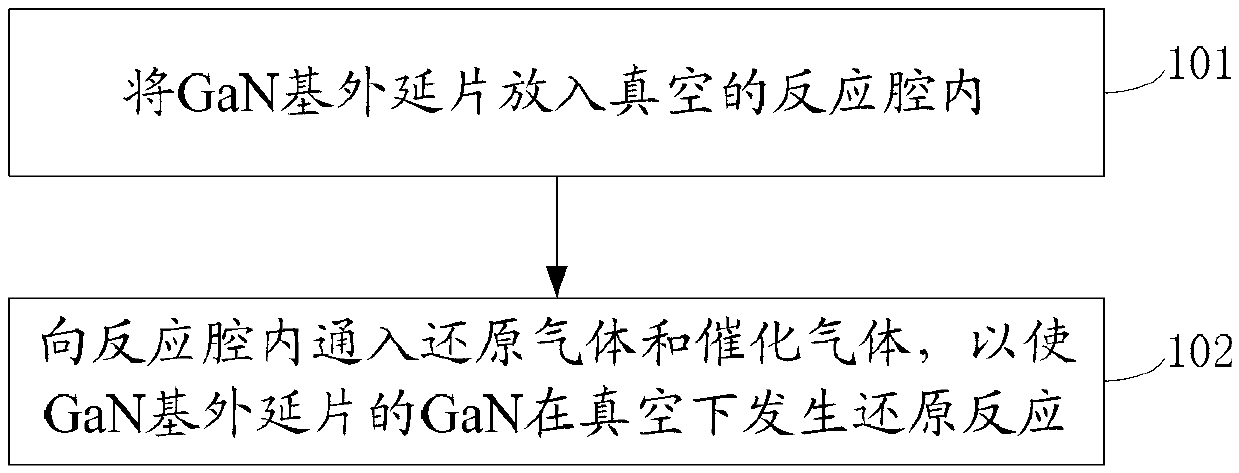
[0023] The embodiment of the present invention provides a method for recovering GaN-based epitaxial wafer substrates, see figure 1 , the method includes:

[0024] Step 101: Put the GaN-based epitaxial wafer into a vacuum reaction chamber.

[0025] Specifically, a GaN-based epitaxial wafer generally includes a substrate, and an n-type GaN layer, a multi-quantum well layer and a p-type GaN layer sequentially stacked on the substrate.

[0026] Specifically, the substrate may be an aluminum oxide substrate or a silicon carbide substrate.

[0027] Step 102: Feed reducing gas and catalytic gas into the reaction chamber, so that the GaN on the GaN-based epitaxial wafer undergoes a reduction reaction under vacuum.

[0028] Specifically, in this embodiment, the reducing gas may be hydrogen.

[0029] Specifically, in this embodiment, the catalytic gas may be hydrogen chloride gas.

[0030] Specifically, the reaction temperature of the reduction reaction is 900°C to 1100°C.

[0031]...


PUM


Abstract

The invention discloses a recovery method of a gyrocompass automatic navigation (GaN)-based epitaxial wafer substrate and belongs to the technical field of semiconductors. The recovery method of the GaN-based epitaxial wafer substrate comprises the following steps: putting the GaN-based epitaxial wafer substrate into a vacuum reaction chamber; and injecting reducing gas and catalytic gas to the reaction chamber so that a reduction reaction of the GaN of the GaN-based epitaxial wafer substrate can occur in vacuo. Due to the facts that the GaN-based epitaxial wafer substrate is put into the vacuum reaction chamber and the reducing gas and the catalytic gas are injected to the reaction chamber so that the reduction reaction of the GaN of the GaN-based epitaxial wafer substrate can occur, the GaN of the GaN-based epitaxial wafer substrate can be reduced to simple substance gallium and ammonia and separated from the substrate. The recovery method of the GaN-based epitaxial wafer substrate has the advantages that no physical damage and chemical damage exist under a high-temperature environment and the integrity of the substrate is maintained. Moreover, the recovery method of the GaN-based epitaxial wafer substrate further has the advantages of being simple in principle, controllable in process, and capable of enabling the decomposition speed rate of the GaN to be higher, and therefore the speed of the recovery of the substrate is improved.

Description

technical field [0001] The invention relates to the technical field of semiconductors, in particular to a method for recycling GaN-based epitaxial wafer substrates. Background technique [0002] With the rapid development of optoelectronic industries such as light-emitting diodes and photodetectors, the production capacity of GaN-based epitaxial wafers based on substrates such as aluminum oxide or silicon carbide has increased unprecedentedly. When growing GaN-based epitaxial wafers, the appearance or photoelectric parameters of some epitaxial wafers cannot meet the requirements of subsequent production, and they need to be scrapped or downgraded. Since the substrate material accounts for a considerable proportion in the cost of epitaxial wafers, the industry is emerging to recycle the substrates of scrapped epitaxial wafers. [0003] Traditional GaN-based epitaxial wafer substrate recovery methods generally include dry etching and wet etching. The dry etching method gener...

Claims


Application Information

Patent Timeline
IPC IPC(8): H01L21/02
Inventor 皮智华刘榕张建宝
Owner HC SEMITEK ZHEJIANG CO LTD
Why Eureka
Try Eureka