Manufacturing method of high dielectric layer metal gate

A technology of high dielectric layer and manufacturing method, which is applied in the direction of semiconductor devices, can solve the problem of reducing the height of metal gates, and achieve the effect of increasing height, compensating losses, and ensuring height

Active Publication Date: 2016-03-30
SEMICON MFG INT (SHANGHAI) CORP
View PDF6 Cites 0 Cited by
  • Summary
  • Abstract
  • Description
  • Claims
  • Application Information

AI Technical Summary

Problems solved by technology

[0005] The invention provides a method for manufacturing a metal gate with a high dielectric layer, which solves the problem in the prior art that the height of the metal gate is reduced due to the removal of pseudo-polysilicon by dry etching and the loss of the interlayer insulating layer in the subsequent process

Method used


Image

  • Manufacturing method of high dielectric layer metal gate
  • Manufacturing method of high dielectric layer metal gate
  • Manufacturing method of high dielectric layer metal gate

Examples


Embodiment Construction

[0031] The principles and features of the present invention are described below in conjunction with the accompanying drawings, and the examples given are only used to explain the present invention, and are not intended to limit the scope of the present invention.

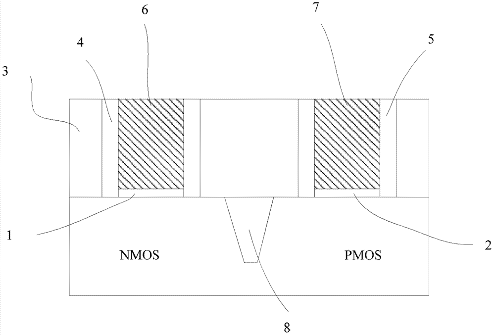
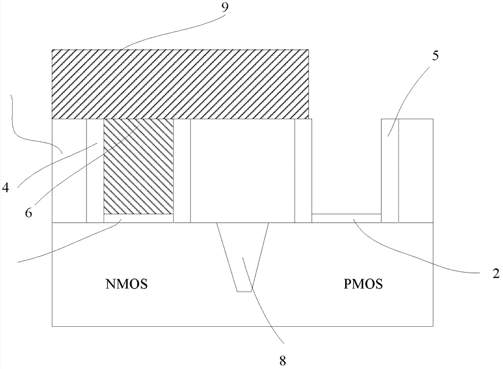
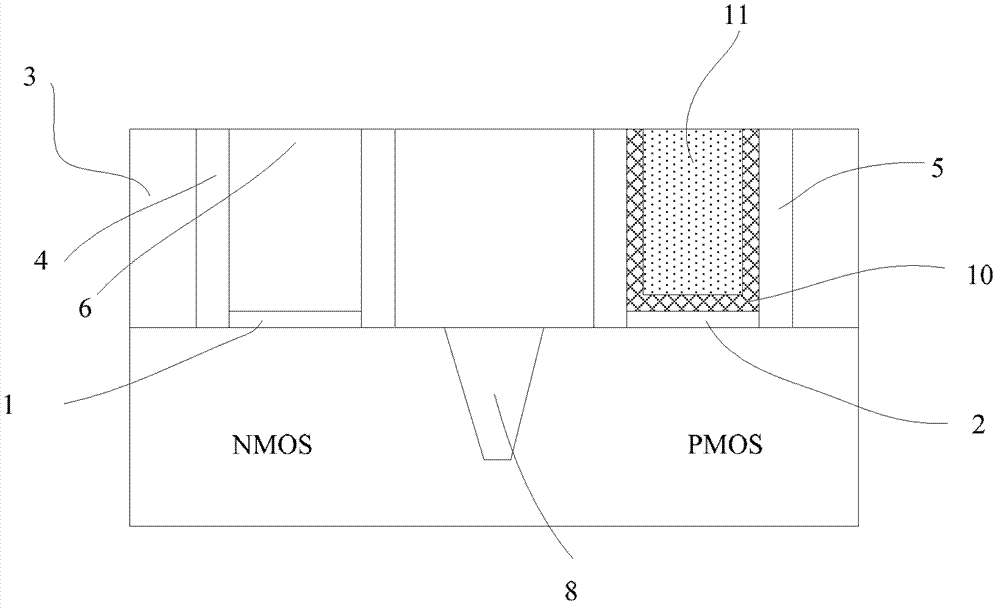
[0032] The technical means adopted in the present invention are realized based on the following concepts. In order to solve the problem of the reduction of the height of the metal gate caused by the loss of the interlayer insulating layer caused by the removal of pseudo-polysilicon by dry etching and the subsequent chemical mechanical polishing process, it is necessary to increase the interlayer insulation The thickness of the layer compensates for the loss caused by dry etching and chemical mechanical polishing.

[0033] Plasma-enhanced chemical vapor deposition using silane to form a seed layer on which selective chemical vapor deposition using ozone and tetraethylorthosilicate can achieve selective deposition, suc...


PUM


Abstract

The invention provides a manufacturing method of a high dielectric layer metal gate. Silane can be utilized to enable plasma to enhance a chemical vapor deposition to form a seed layer. Ozone and tetraethoxysilane can be used for choosing the chemical vapor deposition on the seed layer so as to achieve a first sacrificial layer in selective deposition on the seed layer. The first sacrificial layer can be composited with a second depositional sacrificial layer to increase the height of an interlayer insulation layer changeably and make up the loss of the interlayer insulation layer because of dry etching and subsequent chemical machinery lapping, and then the height of a metal grid which is finally generated can be guaranteed.

Description

technical field [0001] The invention relates to the field of semiconductor device manufacturing, in particular to a method for manufacturing a high dielectric metal gate (HKMG). Background technique [0002] With the development of semiconductor integrated circuits, existing semiconductor devices, such as polysilicon gates commonly used in complementary metal oxide semiconductor (CMOS) devices, have gradually revealed the following problems: the effective thickness of the gate insulating layer increases due to gate loss, The dopant easily penetrates into the substrate through the polysilicon gate to cause a change in the threshold voltage, and it is difficult to achieve a low resistance value on a small width. [0003] In order to solve the above problems, semiconductor technology has developed a semiconductor device that replaces the existing polysilicon gate with a metal gate, and uses a high dielectric constant (highk) material as a semiconductor device for the gate insul...

Claims


Application Information

Patent Timeline
Patent Type & Authority Patents(China)
IPC IPC(8): H01L21/28
Inventor 韩秋华张世谋
Owner SEMICON MFG INT (SHANGHAI) CORP
Why Eureka
Try Eureka