Semiconductor structure and forming method thereof

A technology of semiconductor and interconnect structure, applied in the direction of semiconductor devices, semiconductor/solid-state device manufacturing, semiconductor/solid-state device components, etc. And other issues

Active Publication Date: 2013-06-19
SEMICON MFG INT (SHANGHAI) CORP
View PDF4 Cites 6 Cited by
  • Summary
  • Abstract
  • Description
  • Claims
  • Application Information

AI Technical Summary

Problems solved by technology

However, due to the porosity of the porous material, the mechanical strength of the dielectric layer formed by the porous material is low, and it is easily damaged during wafer processing; When the plasma ashing process removes the photoresist or performs chemical mechanical polishing on the ultra-low K dielectric layer, the plasma will cause damage to the exposed ultra-low K dielectric layer; and, when removing the photoresist or plasma etching During the process, the porous material is easy to absorb water vapor, and the water vapor may react with the porous material, so that the ultra-low K dielectric layer with a low dielectric constant is damaged, and the dielectric constant of the ultra-low K dielectric layer increases, affecting The electrical properties of the interconnect structure

Method used


Image

  • Semiconductor structure and forming method thereof
  • Semiconductor structure and forming method thereof
  • Semiconductor structure and forming method thereof

Examples


Embodiment Construction

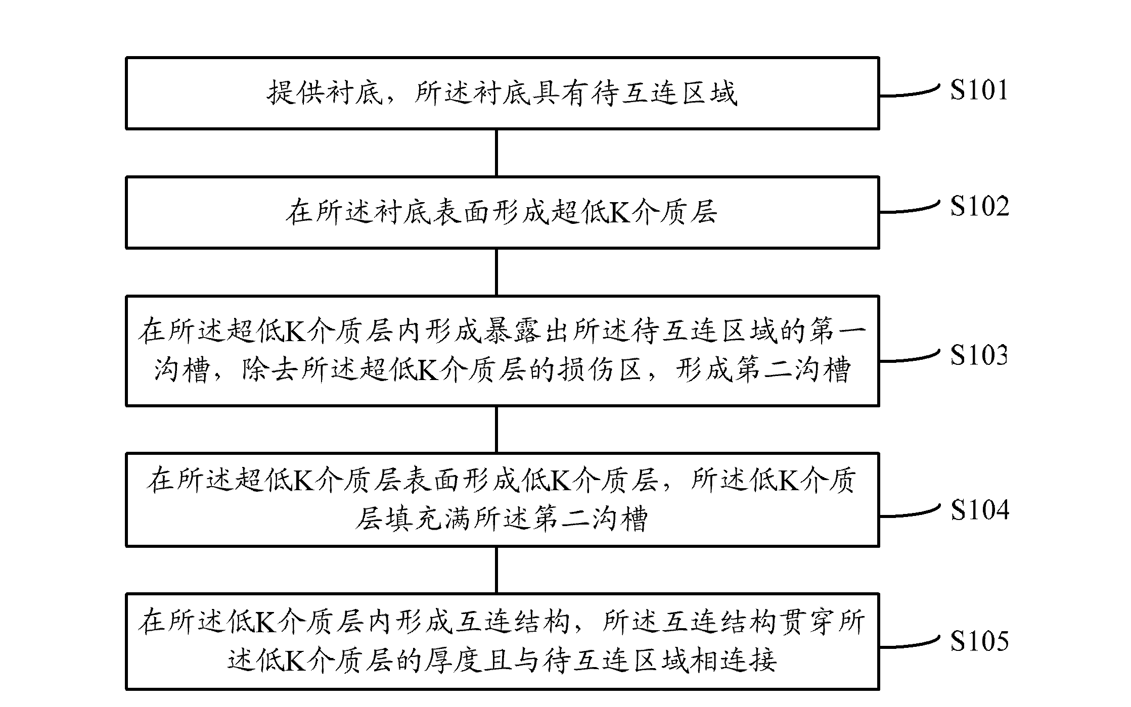
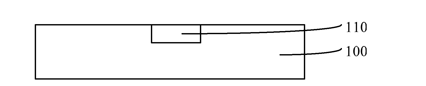
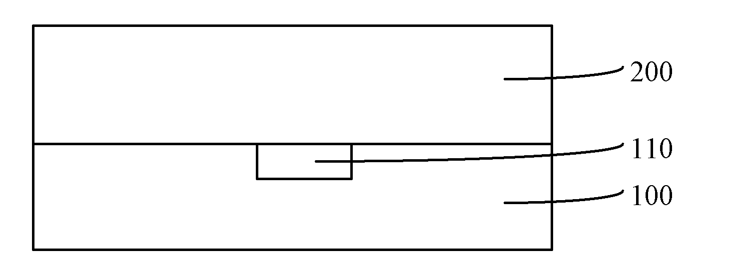
[0035] In the prior art, the ultra-low K dielectric layer is directly subjected to dry etching, chemical mechanical polishing, ashing and other processes, which can easily cause damage to the ultra-low K dielectric layer, making the dielectric constant of the ultra-low K dielectric layer If it becomes larger, the advantages of reducing the crosstalk between metal wirings and reducing the RC delay between metal wiring layers brought by the ultra-low K dielectric layer cannot be utilized. Therefore, the inventor has proposed a semiconductor structure and its formation method after research, and the formation method includes: providing a substrate, the substrate has a region to be interconnected; forming an ultra-low K dielectric layer on the surface of the substrate ; forming a first trench exposing the region to be interconnected in the ultra-low K dielectric layer, removing the damaged region of the ultra-low K dielectric layer to form a second trench; in the ultra-low K dielec...


PUM


Abstract

The invention discloses a semiconductor structure and a forming method thereof. The forming method particularly comprises the steps: providing a substrate which is provided with a to-be-interconnected region; forming an ultralow K medium layer on the surface of the substrate; forming a first groove in the ultralow K medium layer, removing a damage zone of the ultrlow K medium layer and forming a second groove, wherein the to-be-interconnected region is exposed of the first groove; forming a low K medium layer on the surface of the ultralow K medium layer, and filling the second groove by the low K medium layer; and forming an interconnection structure in the low K medium layer, wherein the interconnection structure penetrates through the thickness of the low K medium layer and is connected with the to-be-interconnected region. Due to the fact that the damage zone is removed, the damage zone cannot affect a dielectric constant of the ultralow K medium layer, the low K medium layer is formed in the second groove, the interconnection structure is formed in the low K medium layer subsequently, and a dielectric constant of a whole medium layer is not affected.

Description

technical field [0001] The invention relates to semiconductor manufacturing technology, in particular to a semiconductor structure for interconnection process and its forming method. Background technique [0002] With the continuous development of semiconductor integrated circuit technology, the size of semiconductor devices and the size of interconnection structures are continuously reduced, resulting in the gradual reduction of the spacing between metal wirings, and the dielectric layer used to isolate metal wirings is becoming more and more Thinner and thinner, this will cause crosstalk between metal connections. Now, by reducing the dielectric constant of the dielectric layer between the metal wiring layers, this crosstalk can be effectively reduced, and the low-K dielectric layer can effectively reduce the resistance-capacitance delay (RC delay) between the metal wiring layers, so , low-K dielectric materials and ultra-low-K dielectric materials have been more and more...

Claims


Application Information

Patent Timeline
Patent Type & Authority Applications(China)
IPC IPC(8): H01L21/768H01L23/522
Inventor 邓浩张彬
Owner SEMICON MFG INT (SHANGHAI) CORP
Why Eureka
Try Eureka