Encapsulation structure of silicon substrate pinboard

A packaging structure and adapter board technology, applied in the direction of electrical components, electrical solid devices, circuits, etc., can solve the problems of incomplete insulation layer coverage, high cost of packaging technology, slow speed, etc., to solve process problems and cost problems, The effect of improving product yield and reliability and reducing product cost

Active Publication Date: 2013-06-19
JIANGYIN CHANGDIAN ADVANCED PACKAGING CO LTD
View PDF8 Cites 4 Cited by
  • Summary
  • Abstract
  • Description
  • Claims
  • Application Information

AI Technical Summary

Problems solved by technology

[0003] Through-silicon via interconnection technology has also been applied to the packaging of silicon-based interposers. The formation of through-silicon vias mainly adopts the "BOSCH" etching method, that is, the etching and passivation processes are alternately used. The "BOSCH" etching method will eventually be The ups and downs (scallop) are left on the hole wall, that is, the hole wall corrugation, such as figure 1 As shown, the "BOSCH" alternate etching method is not only slow, but also the corrugation of the hole wall causes incomplete coverage of the insulating layer formed by the subsequent PECVD (plasma enhanced vapor deposition)
At the same time, in the packaging process of silicon-based interposers, the CMP (chemical mechanical polishing) process is commonly used to level the surface and expose the bottom of the metal in the through hole. During this polishing process, the metal or metal ions often migrate, making the Device leakage, resulting in product failure
The above factors have led to high cost and low product yield of the existing silicon-based interposer packaging technology

Method used


Image

  • Encapsulation structure of silicon substrate pinboard
  • Encapsulation structure of silicon substrate pinboard
  • Encapsulation structure of silicon substrate pinboard

Examples


Embodiment Construction

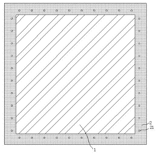
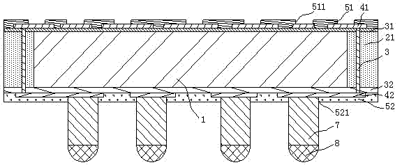
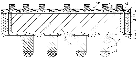
[0041] see Figure 2 to Figure 5 , The packaging structure of a silicon-based interposer in the present invention includes a silicon-based carrier 1, an insulating layer, a rewiring metal layer and a protective layer. An encapsulation area 2 is provided around the silicon-based carrier 1 , and the encapsulation area 2 is in encapsulation connection with the side of the silicon-based carrier 1 . The material of the encapsulation area 2 is resin, usually an epoxy resin material, which contains fillers to reduce the problem of a large difference in thermal expansion coefficient between the resin material and the silicon material, and improve the thermomechanical reliability of the structure. The encapsulation connection can be stepped, and single or multiple steps are used to increase the bonding area between the encapsulation material and the silicon-based carrier 1, thereby improving the bonding force between the encapsulation area 2 and the silicon-based carrier 1, as figure...


PUM


Abstract

The invention relates to an encapsulation structure of a silicon substrate pinboard and belongs to the technical field of semiconductor encapsulation. The encapsulation structure of the silicon substrate pinboard comprises a silicon substrate carrier (1), an encapsulation region (2), a front insulation layer (31), a back insulation layer (32), a front re-wiring metal layer (41), a back re-wiring metal layer (42), a front protective layer (51) and a back protective layer (52). The encapsulation region (2), the front insulation layer (31), the back insulation layer (32), the front re-wiring metal layer (41), the back re-wiring metal layer (42), the front protective layer (51) and the back protective layer (52) are arranged on the periphery of the silicon substrate carrier (1) and are respectively and sequentially arranged on the front and the back of the silicon substrate carrier (1) and the front and the back of the encapsulation region (2). A through hole (21) for filling metal is formed in the encapsulation region (2), and the front re-wiring metal layer (41) is connected with the back re-wiring metal layer (42) through metal in the through hole (21). The encapsulation structure of the silicon substrate pinboard is simple in encapsulation structure, low in encapsulation cost and high in product yield.

Description

technical field [0001] The invention relates to a package structure of a silicon-based adapter plate, which belongs to the technical field of semiconductor package. Background technique [0002] With the development of semiconductor technology, through-silicon via interconnection technology has become a common method for semiconductor packaging. Through-silicon via interconnection technology usually includes the fabrication of through-silicon vias, PECVD (plasma enhanced vapor deposition) technology to form insulating layers, and metal filling, which greatly increases the flexibility of semiconductor packaging. [0003] Through-silicon via interconnection technology has also been applied to the packaging of silicon-based interposers. The formation of through-silicon vias mainly adopts the "BOSCH" etching method, that is, the etching and passivation processes are alternately used. The "BOSCH" etching method will eventually be The ups and downs (scallop) are left on the hole ...

Claims


Application Information

Patent Timeline
Patent Type & Authority Applications(China)
IPC IPC(8): H01L23/492
CPCH01L2224/11
Inventor 张黎赖志明陈栋陈锦辉
Owner JIANGYIN CHANGDIAN ADVANCED PACKAGING CO LTD
Why Eureka
Try Eureka