Electro-static discharge (ESD) protective circuit

An ESD protection and circuit technology, applied in the direction of circuits, electrical components, electric solid devices, etc., can solve the problems of poor anti-ESD ability, limit the application range, affect the discharge ability, etc., achieve small leakage current, suppress latch-up effect, The effect of strong anti-ESD ability

Active Publication Date: 2013-06-19
BEIJING MXTRONICS CORP +1
View PDF3 Cites 5 Cited by
  • Summary
  • Abstract
  • Description
  • Claims
  • Application Information

AI Technical Summary

Problems solved by technology

The gate-grounded NMOS transistor is the most commonly used electrostatic protection circuit, but its anti-ESD ability per unit area is poor, and the layout area required to obtain high ESD protection ability is too large; the CDS transistor has a simple structure, strong clamping ability, and small parasitic capacitance. However, the Darlington effect will appear in the CMOS process, which affects its discharge capability; the SCR tube has strong ESD resistance per unit area and low leakage current, but its unique snapback characteristics are likely to cause latch-up failure. occur
[0004] like figure 1 Shown is a traditional cascaded diode, with 2 N wells on a P substrate, each with a P+ diffused active area and an N+ diffused active area, the cascaded diode closest to

Method used


Image

  • Electro-static discharge (ESD) protective circuit
  • Electro-static discharge (ESD) protective circuit
  • Electro-static discharge (ESD) protective circuit

Examples


Embodiment Construction

[0019] Below in conjunction with accompanying drawing and specific embodiment the present invention is described in further detail:

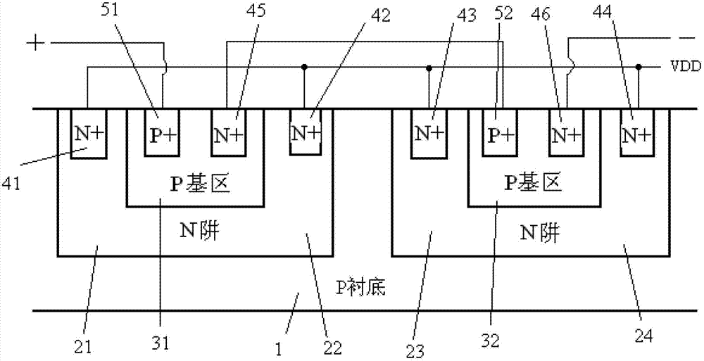
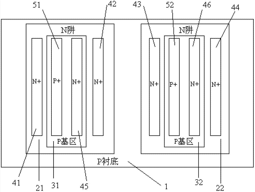
[0020] Such as figure 2 Shown is the schematic diagram of the cross-sectional structure of the ESD protection circuit of the present invention figure 1 , image 3 Shown is the structural representation of the ESD protection circuit of the present invention figure 2 ( figure 2 It can be seen from the figure that the ESD protection circuit of the present invention is a diode string structure that can suppress the Darlington effect, wherein one end of the P substrate 1 is provided with a first N well 21 and a second N well connected at the bottom 22, a first P base region 31 is provided between the first N well 21 and the second N well 22; the other end of the P substrate 1 is provided with a third N well 23 and a fourth N well 24 whose bottoms are integrated, A second P base region 32 is provided between the third N well 23 and the fourth N...


PUM


Abstract

The invention relates to an electro-static discharge (ESD) protective circuit. The ESD protective circuit is in a diode series structure which is capable of restraining a Darlington effect. According to the ESD protective circuit, two ends of a P substrate are respectively provided with two N traps, wherein the bottoms of each two traps are connected into a whole. A P base region is arranged between each two N traps. Each N trap of four N traps is provided with an N+ diffusion active region. Each P base region is provided with a P+ diffusion active region and an N+ diffusion active region. Four of N+ diffusion active regions are connected through wires, and then are connected with power source potential voltage drain drain (VDD). A first P+ diffusion active region is connected with an electricity positive electrode. A fifth N+ diffusion active region is connected with a second P+ diffusion active region through wires. A sixth N+ diffusion active region is connected with an electricity negative electrode. The ESD protective circuit has the advantages of greatly reducing currents flowing to the P substrate, and being capable of effectively restraining the Darlington effect, good in clamping capacity, small in leakage current, good in ESD resistant capacity of unit area, and capable of effectively restraining occurrence of a latch-up effect.

Description

technical field [0001] The invention belongs to the technical field of integrated circuits and relates to an improved structure of cascaded diodes used for electrostatic discharge protection of radio frequency circuits, in particular to an ESD protection circuit. Background technique [0002] For integrated circuits, the electrostatic discharge (ESD) process usually only refers to the electrostatic discharge process with a duration of about 150ns caused by an external object touching a certain connection point of the chip. This process will generate very high transient current and transient Voltage (current of tens of amperes or voltage of thousands of volts), the high electric field caused by ESD will break down the gate oxide layer of the input stage in the integrated circuit, which may cause the integrated circuit chip to fail. As the size of MOS transistors in integrated circuits is getting smaller and smaller, the thickness of the gate oxide layer is also getting thinne...

Claims


Application Information

Patent Timeline
IPC IPC(8): H01L27/02
Inventor 李永峰张娜娜
Owner BEIJING MXTRONICS CORP
Why Eureka
Try Eureka