
Circuit board capable of preventing contact of a gold finger and solder

A gold finger and circuit board technology, which is applied in printed circuit, printed circuit, printed circuit manufacturing, etc., can solve the problems of increasing manpower and working hours of manufacturing process workstations, solder mask tape costs, poor tinning efficiency, and increased manufacturing costs. Achieve the effect of reducing manufacturing unit time, increasing production quantity, and avoiding tin sticking

Inactive Publication Date: 2013-06-19
WISTRON CORP
View PDF7 Cites 4 Cited by
  • Summary
  • Abstract
  • Description
  • Claims
  • Application Information

AI Technical Summary

Problems solved by technology

For example, you can increase the frequency (number of times) of printing and wiping in the solder paste printing workstation or improve the wiping mode (wet wiping, dry wiping, vacuum wiping), etc., to improve the bad phenomenon of gold fingers sticking to tin, but if you increase the wiping frequency It will increase the manufacturing unit time (cycle time), thus causing problems such as reducing the production quantity and increasing the manufacturing cost; moreover, it may be possible to reduce the opening size of the steel plate to reduce the chance of tin powder particles bouncing outwards and causing tin staining. It will cause the problem of poor tinning efficiency; in addition, solder mask tape can also be pasted on the gold finger structure, but this method will increase the manpower and man-hours of the manufacturing process workstation and the cost of solder mask tape during the production process, and may also cause The gold finger remains the residual glue when pasting the solder mask tape

Method used


Image

  • Circuit board capable of preventing contact of a gold finger and solder
  • Circuit board capable of preventing contact of a gold finger and solder
  • Circuit board capable of preventing contact of a gold finger and solder

Examples


Embodiment Construction

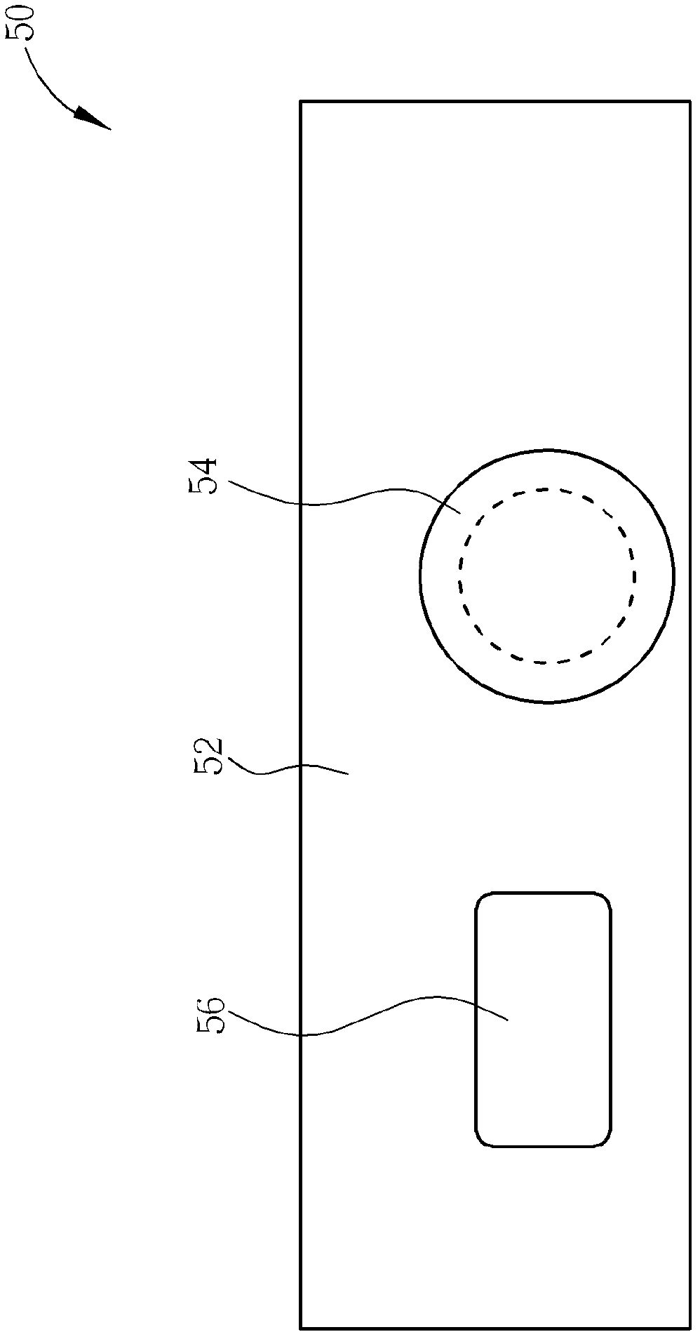
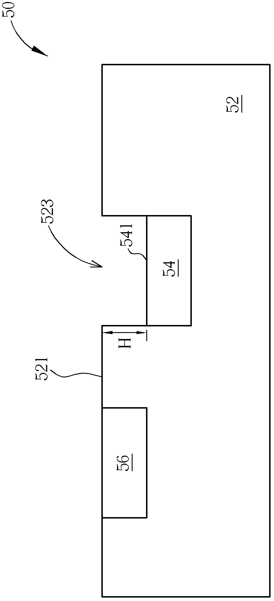
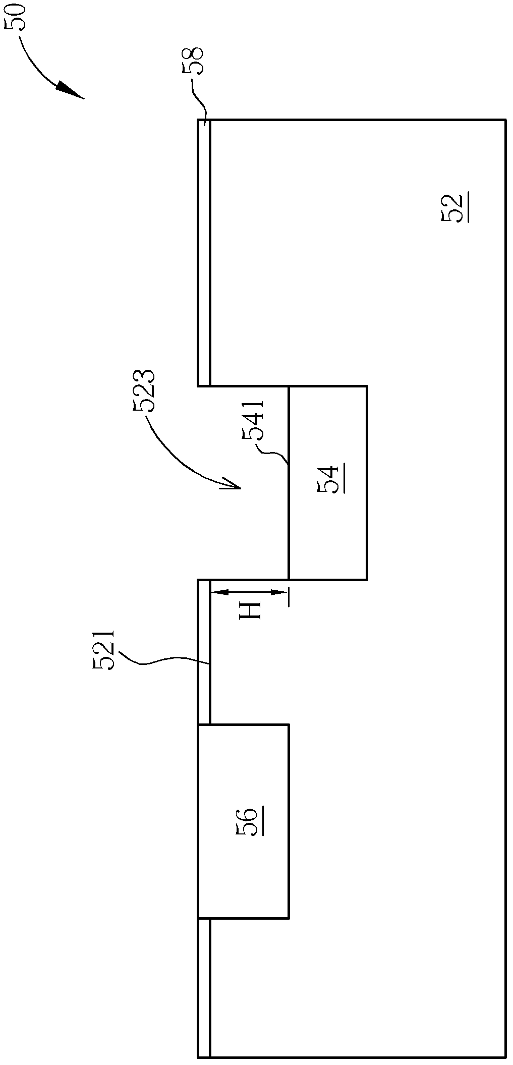
[0025] see figure 1 and figure 2 , figure 1 and figure 2 They are respectively a schematic top view and a schematic cross-sectional view of the circuit board 50 according to Embodiment 1 of the present invention. The circuit board 50 includes a substrate 52, which has a surface 521 and a recess 523 formed thereon; the circuit board 50 further includes a gold finger structure 54, which is arranged in the recess 523 of the substrate 52. There is substantially a height difference H between the top surface 541 and the surface 521 of the substrate 52, wherein the height difference H between the top surface 541 of the gold finger structure 54 and the surface 521 of the substrate 52 can be substantially greater than the particle size of the solder paste particles, for example Generally speaking, the powder particle size of printing solder paste used in the industry is about 20 microns to 38 microns, so the height difference H between the top surface 541 of the gold finger struct...


PUM


Abstract

A circuit board includes a substrate whereon a sunken portion is formed. The circuit board further includes a gold finger structure disposed inside the sunken portion. A height difference is formed between a top surface of the gold finger structure and a surface of the substrate substantially.

Description

technical field [0001] The invention provides a circuit board which can prevent gold fingers from being tinned, especially a circuit board which utilizes the structural design of gold finger settlement to prevent the gold fingers from being tinned. Background technique [0002] In general mobile communication electronic products (such as mobile phones, personal digital assistants, etc.), the circuit boards have gold finger designs, such as gold finger buttons, computer display card slots, and the like. When the golden finger structure of electronic products is stained with tin, it will affect the electrical connection performance, because the activity of tin is much greater than that of gold, so electrochemical reactions will occur during use or storage, such as an insulating oxide layer will be formed on the surface, and serious It affects the transmission of signals. On the other hand, if the surface of the gold finger structure is pure gold-plated, no electrochemical reac...

Claims


Application Information

Patent Timeline
Patent Type & Authority Applications(China)
IPC IPC(8): H05K1/11
CPCH05K1/11H05K3/3485H05K2201/09036H05K2201/09472
Inventor 古振梁李科进
Owner WISTRON CORP
Learn More