A semiconductor device testing device and testing method thereof

A test device and semiconductor technology, applied in the direction of single semiconductor device testing, etc., can solve problems such as affecting test results, ignition, etc., and achieve the effects of accurate test results, simple operation, and little external interference

Active Publication Date: 2016-01-20
南瑞联研半导体有限责任公司
View PDF6 Cites 0 Cited by
  • Summary
  • Abstract
  • Description
  • Claims
  • Application Information

AI Technical Summary

Problems solved by technology

Especially when testing the withstand voltage parameter Vbr, it is necessary to apply high voltage to the table, which is prone to interference such as sparking, which will affect the test results

Method used


Image

  • A semiconductor device testing device and testing method thereof
  • A semiconductor device testing device and testing method thereof
  • A semiconductor device testing device and testing method thereof

Examples


Embodiment

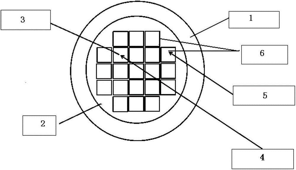
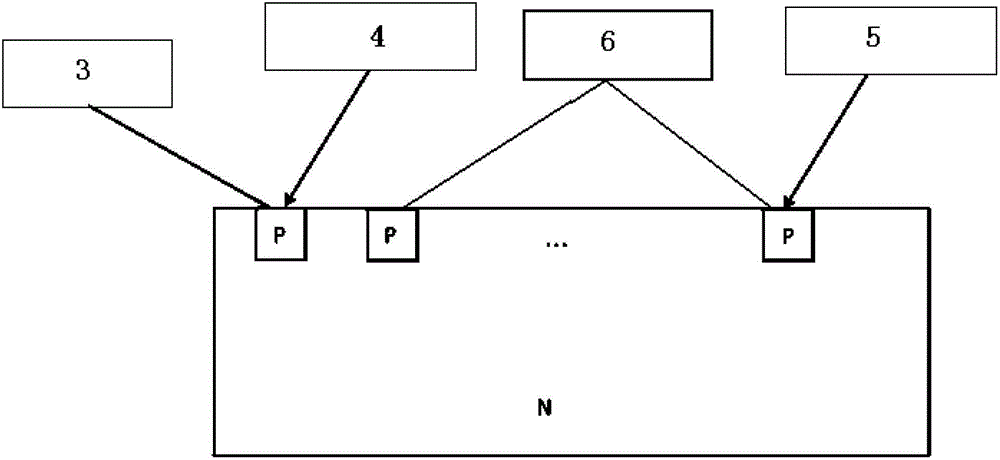
[0039] image 3 It is a test example 1 of the withstand voltage parameter Vbr of the high-voltage fast recovery diode (FRD) of the present invention. The high voltage probe is in contact with any non-test chip, image 3 Shown are the cross-sectional views of the test probe and the high-voltage probe and the chip respectively. Depend on image 3 It can be seen that the wafer is fixed on the table, and the test chip 3 and the non-test chip 6 are selected. The test chip 3 is in contact with the test probe 4, and the potential is grounded. The non-test chip 6 is in contact with the high voltage probe 5 . image 3 In the test example, the high voltage probe 5 applies high voltage, and the test chip 3 is grounded. Test the reverse voltage of the chip 3, that is, the reverse voltage of the P / N junction. In Test Example 1, only the P / N junction forward voltage of 0.7V is introduced. For 1200V or higher voltage devices, the test error is very small, and the test accuracy can be ...


PUM


Abstract

The invention relates to a testing device and a testing method for semiconductor devices. The testing device comprises a testing platform and a probe station, the testing platform comprises a table plate, a circular piece fixed on the table plate, and a semiconductor device arranged on the circular piece, the semiconductor device comprises a testing chip and a non-testing chip, a probe in the probe station comprises a probe contacting with the front of the testing chip and a probe contacting with the silicon surface on the front of the non-testing chip and capable of applying high voltage, and the table plate is a grounded table plate. The testing method includes: fixing the circular piece on the table plate, and selecting the testing chip and the non-testing chip; grounding the table plate; enabling the testing probe to contact with the front of the testing chip, and grounding the testing chip; enabling the high-voltage probe to contact with the silicon surface of the front of the non-testing chip, and applying the high voltage to the testing chip through the high-voltage probe; and reading a voltage and current curve of the testing chip by the testing probe. The high voltage is directly applied on the front of the chip, so that interferences such as sparking are reduced, testing results are accurate, and safety is higher.

Description

technical field [0001] The invention relates to a semiconductor device device and method, in particular to a semiconductor device test device and a test method thereof. Background technique [0002] As freewheeling and rectifying devices, fast recovery diodes are widely used in the field of power electronics. Testing fast recovery diodes at the wafer level becomes difficult when breakdown voltage requirements of 1200V or higher are required. The existing test technology adopts test equipment + probe station, which is connected by cables; the wafer is fixed on the table, and the characteristics of the fast recovery diode are tested by applying an electric bias to the table and the probe. Since the fast recovery diode is a vertical device, it is necessary to set the potential of the plate when testing the characteristics of the fast recovery diode. Especially in the test of the withstand voltage parameter Vbr, it is necessary to apply high voltage to the table, which is pron...

Claims


Application Information

Patent Timeline
Patent Type & Authority Patents(China)
IPC IPC(8): G01R31/26
Inventor 刘江王耀华刘钺杨赵哿高明超金锐
Owner 南瑞联研半导体有限责任公司
Why Eureka
Try Eureka