

Solid-liquid interdiffusion bonding structure of thermoelectric module and fabricating method thereof
A technology of diffusion bonding and thermoelectric modules, which is applied in the manufacture/processing of thermoelectric devices, the material of the junction lead wires of thermoelectric devices, and the manufacturing tools, etc., which can solve the problems of high temperature of the bonding process and damage to the bonding interface.
- Summary
- Abstract
- Description
- Claims
- Application Information
AI Technical Summary
Problems solved by technology
Method used
Image

Examples
example 1
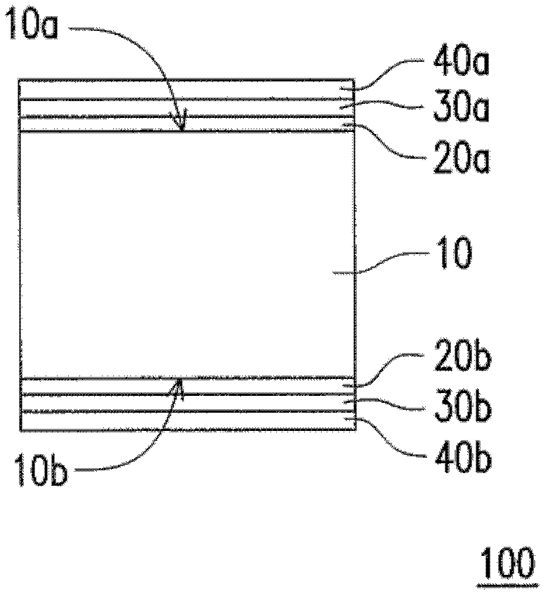
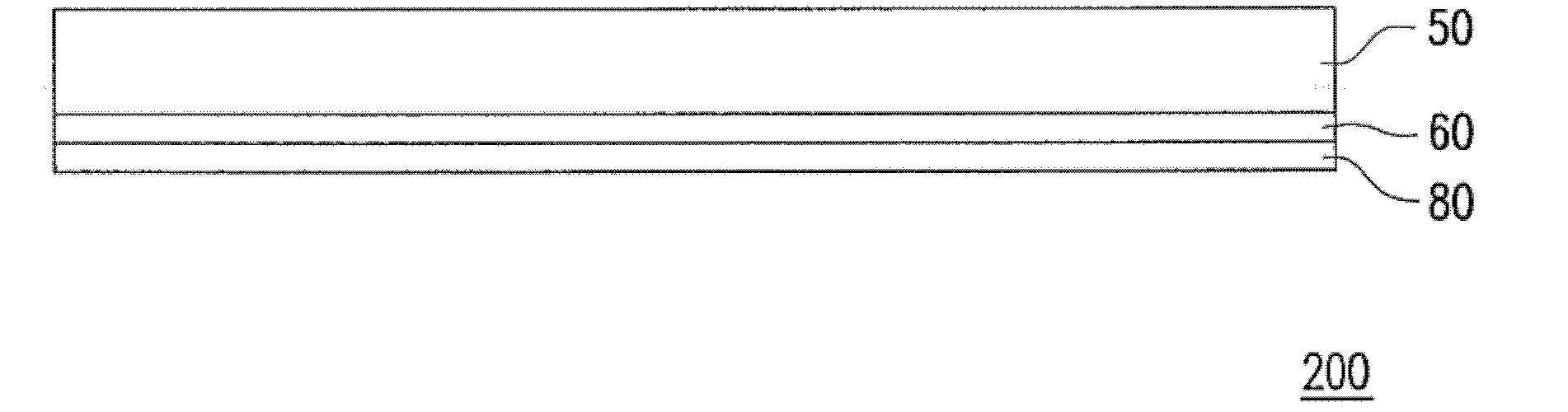
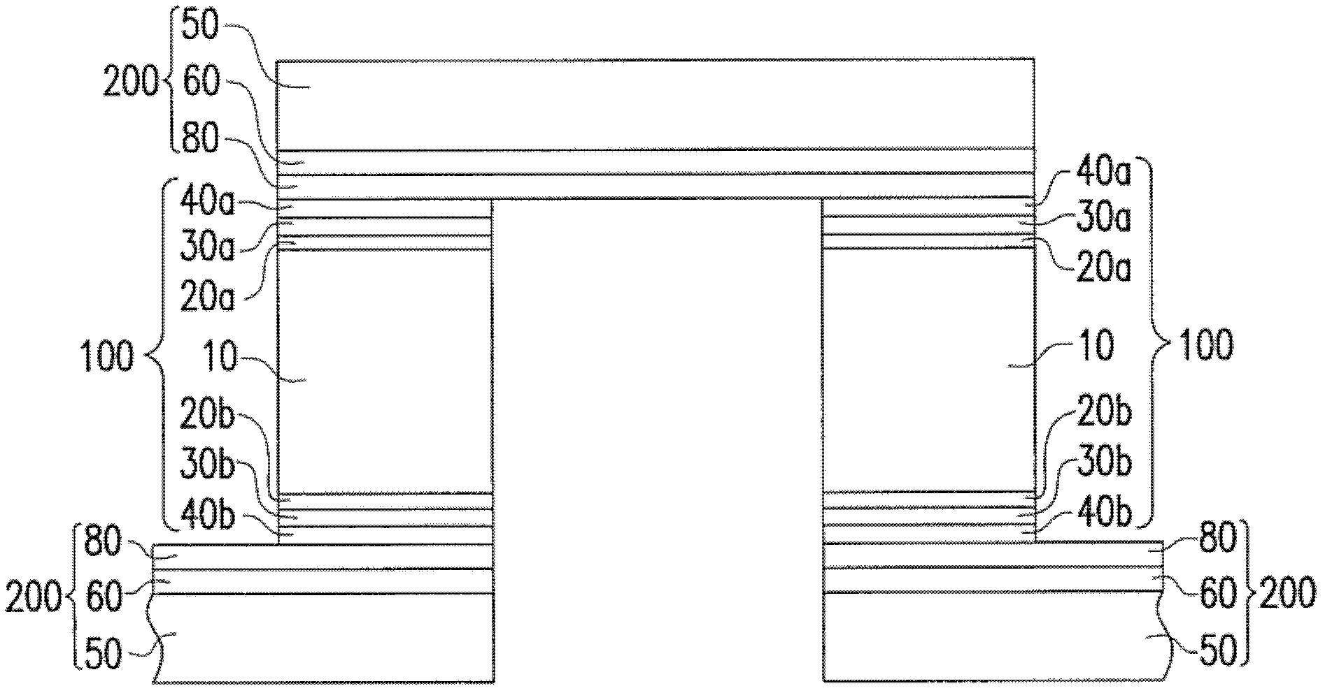
[0042] The bonding method of the thermoelectric module of Example 1 is in the P-type thermoelectric element (Bi 0.5 Sb 1.5 Te 3 ) is sequentially plated with a nickel layer with a thickness of 4 microns and a silver layer with a thickness of 10 microns. In addition, a silver layer with a thickness of 2 microns and a tin layer with a thickness of 4 microns were sequentially plated on the surface of the copper electrode plate. Afterwards, the thermoelectric element formed with the nickel layer and the silver layer and the copper electrode plate formed with the silver layer and the tin layer are stacked together, and a heating process is performed in a vacuum or an inert gas environment. The temperature of the heating program is 300 degrees centigrade, and the time is 30 minutes. At this time, the tin layer on the copper electrode plate will melt and quickly carry out interface reaction with the silver layer on the copper electrode plate and the silver layer on the thermoelectr...
example 2
[0045] The joining method of the thermoelectric module of example two is in the N-type thermoelectric element (Bi 2 Te 2.55 Se 0.45 ) is sequentially plated with a tin layer with a thickness of 2 microns, a nickel layer with a thickness of 4 microns, and a silver layer with a thickness of 10 microns. In addition, a silver layer with a thickness of 2 microns and a tin layer with a thickness of 4 microns were sequentially plated on the surface of the copper electrode plate. Afterwards, the thermoelectric element formed with the tin layer, the nickel layer and the silver layer and the copper electrode plate formed with the silver layer and the tin layer are stacked together, and a heating process is performed in a vacuum or an inert gas environment. The temperature of the heating program is 300 degrees centigrade, and the time is 30 minutes. At this time, the tin layer on the copper electrode plate will melt and quickly carry out interface reaction with the silver layer on the ...
example 3
[0048] The bonding method of the thermoelectric module of Example 3 is first in the P-type thermoelectric element (Pb 0.5 sn 0.5 The surface of Te) is sequentially plated with a tin layer with a thickness of 2 microns, a nickel layer with a thickness of 4 microns and a silver layer with a thickness of 10 microns. In addition, a silver layer with a thickness of 2 microns and a tin layer with a thickness of 4 microns were sequentially plated on the surface of the copper electrode plate. Afterwards, the thermoelectric element formed with the nickel layer and the silver layer and the copper electrode plate formed with the silver layer and the tin layer are stacked together, and a heating process is performed in a vacuum or an inert gas environment. The temperature of the heating program is 300 degrees centigrade, and the time is 30 minutes. At this time, the tin layer on the copper electrode plate will melt and quickly carry out interface reaction with the silver layer on the cop...
PUM
| Property | Measurement | Unit |
|---|---|---|
| Thickness | aaaaa | aaaaa |
| Thickness | aaaaa | aaaaa |
| Thickness | aaaaa | aaaaa |
Abstract
Description
Claims
Application Information