Insulated gate bipolar transistor gate driving push-pull circuit

A technology of bipolar transistors and push-pull circuits, which is applied in the field of gate drive push-pull circuits of insulated gate bipolar transistors, and can solve the problems of large turn-on voltage drop of MOS transistors, poor reliability of push-pull circuits, and poor ability to suppress IGBT short-circuit current, etc. problem, to achieve the effect of small drive circuit loss, improve work reliability, and improve overall reliability

Active Publication Date: 2013-06-26
NANJING ESTUN AUTOMATION CO LTD
View PDF7 Cites 20 Cited by
  • Summary
  • Abstract
  • Description
  • Claims
  • Application Information

AI Technical Summary

Problems solved by technology

[0012] Disadvantages of this topology: (1) The gate clamping effect is poor, and the ability to suppress IGBT short-circuit current is poor
When the peak driving current of the triode is large, the CE voltage drop becomes higher, and there is also a certain saturation voltage drop when it is saturated and turned on.
However, the indirect consequences of higher power supply are that the gate clamping effect of the driving circuit is poor, the short-circuit current of the driven IGBT is greatly increased, and the risk of IGBT damage increases
(2) There is a possibility of through-through inside the push-pull structure
There may be a direct connection between the push-pull upper and lower tubes, resulting in instantaneous saturation of the switching power supply, affecting the power supply of the entire system, and greatly reducing system reliability.
(3) Large loss
There is a saturation voltage drop of 0.7V when the triode is saturated and turned on. When it is used to drive the push-pull stage, the loss is relatively large, especially in the case of high switching frequency, the heat is obvious
[0015] Disadvantages of this topology: (1) The gate clamping effect is poor, and the ability to suppress IGBT short-circuit current is poor
When the peak driving current of the triode is large, the CE voltage drop becomes higher, and there is also a certain saturation voltage drop when it is saturated and turned on.
This phenomenon is very harmful and can easily cause irreversible damage to the system.
(3) Large loss
There is a saturation voltage drop of 0.7V when the triode is saturated and turned on. When it is used to drive the push-pull stage, the loss is relatively large, especially in the case of high switching frequency, the heat is obvious
[0018] Disadvantages of this topology: (1) MOS tube GS voltage is too high
The MOS tube GS has to withstand the voltage of ±23V, which exceeds ±20V, which cannot be achieved by general MOS tubes, and special MOS tubes must be purchased
(2) The GS voltage of the push-pull MOS tube will be affected by the gate voltage of the IGBT
When the gate voltage rises, as the G-point voltage of the IGBT rises, the GS voltage of the upper MOS transistor gradually decreases, and the conduction voltage drop of the MOS transistor increases, resulting in an IGBT gate voltage of about 11V, which is much lower than 15V, and the IGBT cannot be completely opened
(3) There is a possibility of through-through inside the push-pull structure
[0021] Disadvantages of this topology: (1) MOS tube GS voltage is too high
[0023] The following technical problems generally exist in the triode push-pull topology: (1) The gate clamping effect is poor, and the IGBT short-circuit current suppression ability is poor; (2) The loss is large; (3) There may be a through-through inside the push-pull structure, and the overall system reliability is poor
[0024] The MOS tube push-pull topology generally has the following technical problems: (1) MOS tube GS voltage is higher than ±20V, and the reliability of the push-pull circuit is poor; (2) There may be a through-through inside the push-pull structure, and the overall system reliability is poor; (3) MOS tube The GS voltage may be affected by the gate voltage of the driven IGBT, resulting in excessive conduction voltage drop of the MOS transistor
[0025] Generally speaking, the triode push-pull topology cannot achieve effective gate clamping, causing the driven IGBT to be easily damaged when a short circuit occurs, while the MOS tube push-pull topology MOS tube itself is easily damaged, resulting in poor overall system reliability.

Method used


Image

  • Insulated gate bipolar transistor gate driving push-pull circuit
  • Insulated gate bipolar transistor gate driving push-pull circuit
  • Insulated gate bipolar transistor gate driving push-pull circuit

Examples


Embodiment Construction

[0055] The present invention will be described in further detail below in conjunction with the accompanying drawings and embodiments.

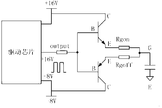
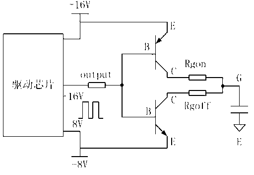
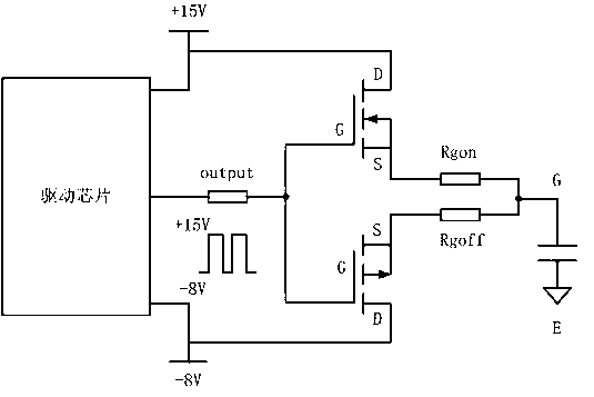
[0056] Figure 5 It is a schematic diagram of the structure of the IGBT drive push-pull circuit with effective gate clamping and negative voltage shutdown of the present invention, which is composed of a drive chip, an IGBT gate drive resistor, and a gate drive push-pull circuit. The gate drive push-pull circuit is composed of a front-stage push-pull circuit, a level conversion circuit, and a rear-stage push-pull circuit. The front-stage push-pull circuit, the level conversion circuit and the rear-stage push-pull circuit share the positive and negative power supplies of the secondary side of the drive chip. The output of the driver chip is connected to the front-stage push-pull circuit, the output of the front-stage push-pull circuit is connected to the level conversion circuit, the output of the level conversion circuit is connected to the r...


PUM


Abstract

The invention discloses an insulated gate bipolar transistor (IGBT) gate driving push-pull circuit. The IGBT gate driving push-pull circuit is powered by a positive-negative power supply of a driving chip secondary side, and output positive-negative level. A pre-push-pull circuit, a level converting circuit and a post-push-pull circuit share the positive-negative power supply of the driving chip secondary side. The output of the driving chip is connected with the input of the pre-push-pull circuit; the output of the pre-push-pull circuit is connected with the level converting circuit; the output of the level converting circuit is connected with the post-push-pull circuit; and the output of the post-push-pull circuit is connected with a gate driving resistor of the IGBT. The pre-push-pull circuit is combined with the level converting circuit to provide a driving signal of interlocking and a hardware dead zone for MOS (metal oxide semiconductors) of the post-push-pull circuit, so that direct communications of the interior of the MOS push-pull structure is avoided; and GS voltage of the MOS is limited in a range of + / - 20V, so that reliable operation of the MOS is guaranteed. Adopting the MOS, the post-push-pull circuit can cooperate with effective IGBT gate clamps to limit IGBT short-circuit currents, and improve operation reliability of the IGBT.

Description

technical field [0001] The invention relates to an insulated gate bipolar transistor gate driving push-pull circuit, in particular to an insulated gate bipolar transistor gate driving push-pull circuit cooperating with effective gate clamping negative voltage shutdown. Background technique [0002] The so-called insulated gate bipolar transistor (Insolated Gate Bipolar Transistor, IGBT) gate clamping refers to clamping the gate voltage of the insulated gate bipolar transistor (IGBT) through circuit design, that is: when there is an external effect, such as a short circuit causes the IGBT When the gate voltage is raised passively, the gate voltage is kept stable through circuit design. This is an essential function to ensure the reliable operation of the IGBT. [0003] When the IGBT is short-circuited, Ic increases sharply due to the presence of Miller capacitance (see Figure 9 ), in this process, the IGBT gate potential tends to rise, and this effect comes from the collect...

Claims


Application Information

Patent Timeline
Patent Type & Authority Applications(China)
IPC IPC(8): H02M1/088
Inventor 姚瑱戴安刚郑静文吴波
Owner NANJING ESTUN AUTOMATION CO LTD
Why Eureka
Try Eureka