
Silicon wafer thinning fixture with through-hole electroplating copper salient points and thinning technique

A technology of through-hole electroplating and process method, which is applied in the manufacturing of circuits, electrical components, semiconductor/solid-state devices, etc., can solve problems such as cracks, wafer ruptures, stress concentration, etc., to achieve low cost, improve yield, and avoid stress concentration. Effect

Active Publication Date: 2013-07-03
刘胜
View PDF3 Cites 5 Cited by
  • Summary
  • Abstract
  • Description
  • Claims
  • Application Information

AI Technical Summary

Problems solved by technology

During the electroplating of the through-hole of the silicon wafer, it is very easy to form copper bumps at the through-holes of the silicon wafer. During the thinning process of the wafer, it is easy to cause stress concentration at the position of the bump, which in turn causes cracks and even rupture of the wafer.

Method used


Image

  • Silicon wafer thinning fixture with through-hole electroplating copper salient points and thinning technique
  • Silicon wafer thinning fixture with through-hole electroplating copper salient points and thinning technique
  • Silicon wafer thinning fixture with through-hole electroplating copper salient points and thinning technique

Examples


Embodiment 1

[0029] Further illustrate this embodiment below in conjunction with accompanying drawing:

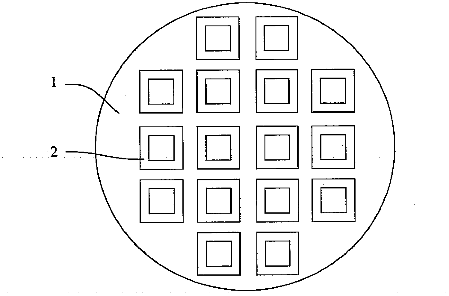
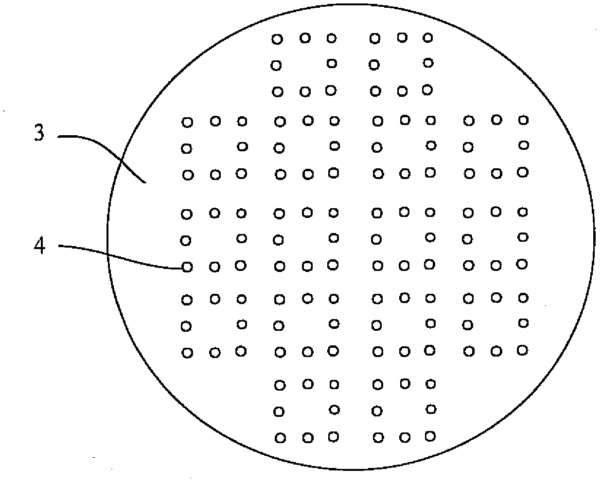
[0030] Referring to the figure, the jig wafer 1 is provided with a groove 2 capable of accommodating copper bumps 4 on the silicon wafer. The material of the jig wafer 1 is a silicon wafer or a metal wafer. Mark for fixture wafer 1 alignment.

[0031] The steps of the thinning process package in this embodiment are as follows:

[0032] A. Electroplating the silicon wafer 3 with through holes. The through holes in the silicon wafer 3 are electroplated in a bottom-up manner. First, the back of the silicon wafer 3 is electroplated, and the through holes on the back are sealed. The sealing process can be partial The hole is sealed by electroplating, and the copper metal 6 filling the through hole is not formed on the back. Due to the influence of the electroplating process, local bumps are easily formed at the opening of the through hole, that is, the protrusion 7 produced by partially fil...

Embodiment 2

[0039] Embodiment 2 is the same as Embodiment 1, except that the fixing method of silicon wafer 3 and fixture wafer 1 is vacuum adsorption, and the silicon wafer 3 and fixture wafer are connected through the vacuum adsorption through hole 10 on the fixture circle 1. 1 fixed, such as Figure 6 shown.

Embodiment 3

[0041] Embodiment 3 is the same as Embodiment 1, except that the fixture disc 1 is made of stainless steel, and the fixture disc 1 is manufactured by machining. The shape of the groove 2 on the fixture disc 1, the processing methods include: corrosion, laser cutting, grinding, milling. In order to ensure the flatness of the fixture disc 1, the fixture disc 1 needs to be polished, such as figure 1 , figure 2 shown.


PUM


Abstract

The invention discloses a silicon wafer thinning fixture with through-hole electroplating copper salient points and a thinning technique. A fixture wafer is provided with grooves capable of containing copper salient points on a thinning silicon wafer, and aligning marks used for the thinning silicon wafer and the fixture wafer are arranged on the fixture wafer. After partial electroplating hole sealing is carried out on the through hole of the silicon wafer, front side porefilling electroplating is carried out, and copper points are formed in the front side of the silicon wafer. According to the distribution of the copper points on the silicon wafer, the grooves are etched in the fixture wafer by adopting etching, corroding or machining, the silicon wafer with the electroplating copper salient points is aligned to and fixed with the fixture wafer by using the aligning marks, and thinning is carried out on the front side and the back side of the silicon wafer by adopting a mechanical grinding process or a chemico-mechanical polishing process. The silicon wafer thinning fixture with the through-hole electroplating copper salient points and the thinning technique have the advantages that stress concentration generated when the copper salient points on the silicon wafer are directly extruded in a thinning process is avoided, the problem that wafer breaking is prone to occurring when the silicon wafer with the through-hole electroplating copper salient points is thinned can be effectively avoided, and the rate of the finished product of the thinning of the silicon wafer is improved.

Description

technical field [0001] The invention relates to semiconductor manufacturing equipment and technology, in particular to a silicon wafer thinning jig with through-hole electroplated copper bumps and a thinning process method. Background technique [0002] Three-dimensional packaging is the development trend of semiconductor packaging technology. Three-dimensional packaging requires through holes to be made on silicon wafers, and metals are filled in the through holes through electroplating, deposition and other processes to achieve vertical electrical interconnection. At the same time, two or more chips need to be stacked for system-level packaging, which requires Thinning the wafer to 100μm or even below 100μm. Wafer thinning is to cut the wafer by mechanical grinding, and mechanical cutting will form a certain thickness of damage layer on the surface of the wafer. The damaged layer on the surface of the wafer can be removed by chemical mechanical polishing process. When t...

Claims


Application Information

Patent Timeline
Patent Type & Authority Applications(China)
IPC IPC(8): H01L21/687H01L21/302
Inventor 刘胜陈照辉汪学方王宇哲
Owner 刘胜
Learn More