Package module of embedded package and manufacturing method of package

A technology for packaging modules and manufacturing methods, which is applied in semiconductor/solid-state device manufacturing, electrical solid-state devices, semiconductor devices, etc., can solve problems such as reduced packaging yield, electrical failure of the overall packaging module, and poor packaging of micro-semiconductor chips. Convenient electrical connection, high-strength effect

Active Publication Date: 2013-07-17
KING YUAN ELECTRONICS
View PDF4 Cites 1 Cited by
  • Summary
  • Abstract
  • Description
  • Claims
  • Application Information

AI Technical Summary

Problems solved by technology

[0004] However, if in the above-mentioned packaging process, several semiconductor chips with large size differences are to be packaged, the packaging yield will be reduced due to the difficulty in uniform control of the manufacturing

Method used


Image

  • Package module of embedded package and manufacturing method of package
  • Package module of embedded package and manufacturing method of package
  • Package module of embedded package and manufacturing method of package

Examples


Embodiment 1

[0040] refer to Figure 1A to Figure 1N , which is a schematic flow chart of manufacturing the package in this embodiment.

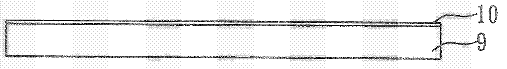
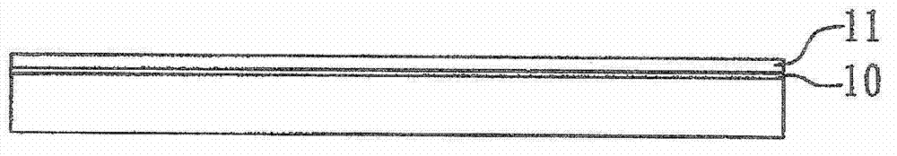
[0041] First, if Figure 1A As shown, a carrier board 9 is provided, and a release film 10 is pasted on the surface of the carrier board 9 . The materials of the release film 10 and the carrier plate 9 are not particularly limited, and materials commonly used in the present invention can be used. Next, if Figure 1B As shown, a conductive layer 11 is pasted on the surface of the release film 10 . In this embodiment, metal copper foil with a thickness of about 18 μm is used as the conductive layer 11 .

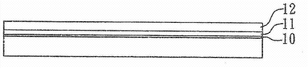
[0042] Such as Figure 1C As shown, a patterned dielectric layer 12 is formed on the surface of the conductive layer 11. The material of the dielectric layer 12 is not particularly limited, and dielectric materials commonly used in the field can be used. Next, a plurality of blind holes 120 are opened in the dielectric layer 12 by using methods such ...

Embodiment 2

[0049] refer to Figure 2A to Figure 2C , which is a schematic flow chart of manufacturing the packaging module in this embodiment.

[0050] First, if Figure 2A As shown, a packaging substrate 30 and a second semiconductor chip 20 are provided, wherein the packaging substrate 30 has a second electrical connection pad 301, and the second semiconductor chip 20 has a second active surface 20a, a second passive surface surface 20b, and a second electrode pad 201 located on the second active surface 20a. A third adhesive film 21 is pasted on the second passive surface 20b of the second semiconductor chip 20 .

[0051] Next, if Figure 2B As shown, the second semiconductor chip 20 is disposed on the surface of the packaging substrate 30 having the second electrical connection pad 301 through the third adhesive film 21 . In addition, a second adhesive film 22 is used to attach between the second surface 1 b of the package 1 prepared in the first embodiment and the second active ...


PUM

PropertyMeasurementUnit
Thicknessaaaaaaaaaa

Abstract

The invention relates to a package module of an embedded package and a manufacturing method of the package. The package comprises a first semiconductor chip, a dielectric layer, a first circuit layer, a second circuit layer and a first packaging material. The package module mainly comprises the package, a second semiconductor chip and a second packaging material. Since the package body is tested and confirmed to have good functions and then can be used in the package module, a problem that the package module cannot be fully made use of due to flaws of the package is prevented.

Description

technical field [0001] The present invention relates to a package module and a package body and a manufacturing method thereof, in particular to a package body (known good die package) which is confirmed to have a good function after testing, a package module embedded with the package body, and its Both methods of manufacture. Background technique [0002] With the vigorous development of the electronic industry, electronic products tend to be thinner and smaller in form, and gradually enter the research and development direction of high-function, high-performance, and high-speed in terms of function. In order to meet the high integration and miniaturization requirements of semiconductor devices, the volume of the embedded semiconductor chip is also miniaturized, so the area of ​​the electrode pad on the semiconductor chip for electrical connection with the outside is also the same. This situation increases the difficulty of electrical connection and packaging of semiconduc...

Claims


Application Information

Patent Timeline
IPC IPC(8): H01L23/498H01L23/31H01L21/60H01L21/56H01L21/683
CPCH01L2224/32225H01L2924/19107H01L2224/48227H01L2224/73215H01L2224/73265
Inventor 林殿方
Owner KING YUAN ELECTRONICS
Why Eureka
Try Eureka