P-type silicon substrate heterojunction cell

A heterojunction cell and silicon substrate technology, applied in the field of solar cells, can solve the problems of reduced light energy conversion efficiency, ineffective carrier collection, reduced transition tunneling probability, etc., and achieves increased processes, increased costs, and increased The effect of collection and utilization

Active Publication Date: 2015-04-15
TRINA SOLAR CO LTD
View PDF3 Cites 0 Cited by
  • Summary
  • Abstract
  • Description
  • Claims
  • Application Information

AI Technical Summary

Problems solved by technology

[0002] At present, using P-type crystalline silicon as the substrate to form heterojunction battery devices generally uses intrinsic type a-Si to passivate the surface of crystalline silicon (substrate), and at the same time add doped p-a-Si:H The back field (BSF) is formed, but due to the large valence band between p-a-Si:H and p-c-Si, the probability of hole transition tunneling in the back field is reduced, so that the carrier cannot be collected effectively. Light energy conversion efficiency is reduced

Method used


Image

  • P-type silicon substrate heterojunction cell
  • P-type silicon substrate heterojunction cell

Examples


Embodiment Construction

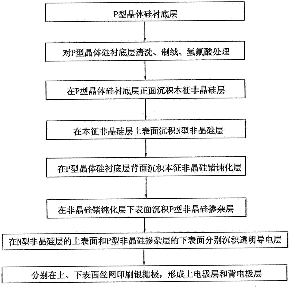
[0019] In order to make the content of the present invention easier to understand clearly, the present invention will be described in further detail below according to specific embodiments in conjunction with the accompanying drawings,

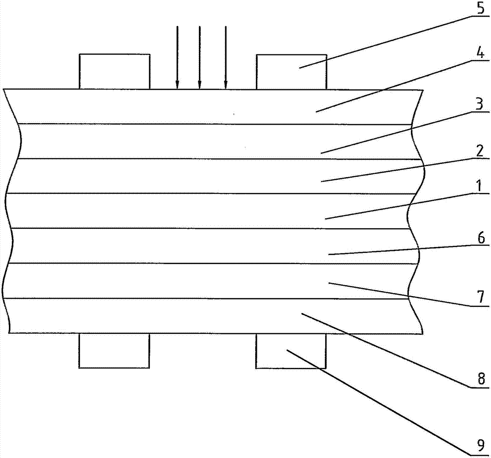
[0020] Such as figure 1 As shown, a P-type silicon substrate heterojunction cell comprises a P-type crystalline silicon substrate layer 1, an intrinsic amorphous silicon layer 2, an N-type amorphous silicon layer 3, and a P-type amorphous silicon layer. Doped layer 7, a first transparent conductive layer 4, an upper electrode layer 5, an intrinsic amorphous silicon germanium passivation layer 6, a second transparent conductive layer 8 and a back electrode layer 9, P-type crystalline silicon lining The bottom layer 1 has a front side and a back side, the intrinsic amorphous silicon layer 2 is deposited on the front side of the P-type crystalline silicon substrate layer 1; the N-type amorphous silicon layer 3 is deposited on the upper surface of...


PUM

PropertyMeasurementUnit
thicknessaaaaaaaaaa
thicknessaaaaaaaaaa
thicknessaaaaaaaaaa

Abstract

The invention discloses a P-type silicon substrate heterojunction cell which comprises a P-type crystalline silicon substrate layer, an intrinsic non-crystalline silicon layer, an N-type non-crystalline silicon layer, a P-type non-crystalline silicon doping layer, a first transparent conducting layer, an upper electrode layer, an intrinsic non-crystalline silicon germanium passivation layer, a second transparent conducting layer and a back electrode layer, wherein the P-type crystalline silicon substrate layer is provided with a front and a back; the intrinsic non-crystalline silicon layer is deposited at the front of the P-type crystalline silicon substrate layer; the N-type non-crystalline silicon layer is deposited on the upper surface of the intrinsic non-crystalline silicon layer; the first transparent conducting layer is located on the upper surface of the N-type non-crystalline silicon layer; the intrinsic non-crystalline silicon germanium passivation layer is deposited at the back of the P-type crystalline silicon substrate layer; the P-type non-crystalline silicon doping layer is deposited on the lower surface of the intrinsic non-crystalline silicon germanium passivation layer; the second transparent conducting layer is located on the lower surface of the P-type non-crystalline silicon doping layer; and the back electrode layer is located on the lower surface of the second transparent conducting layer, and is electrically connected with the P-type non-crystalline silicon doping layer through the second transparent conducting layer. According to the P-type silicon substrate heterojunction cell, the transition probability of a hole at the back of a substrate can be increased; collection and utilization of carriers are increased; a short-circuit current is increased; and the conversion efficiency of the cell is improved.

Description

technical field [0001] The invention relates to a P-type silicon substrate heterojunction cell, which belongs to the technical field of solar cells. Background technique [0002] At present, using P-type crystalline silicon as the substrate to form heterojunction battery devices generally uses intrinsic type a-Si to passivate the surface of crystalline silicon (substrate), and at the same time add doped p-a-Si:H The back field (BSF) is formed, but due to the large valence band between p-a-Si:H and p-c-Si, the probability of hole transition tunneling in the back field is reduced, so that the carrier cannot be collected effectively. Light energy conversion efficiency is reduced. Contents of the invention [0003] The technical problem to be solved by the present invention is to overcome the defects of the prior art and provide a P-type silicon substrate heterojunction cell, which can increase the transition probability of holes on the back of the substrate, increase the col...

Claims


Application Information

Patent Timeline
Patent Type & Authority Patents(China)
IPC IPC(8): H01L31/075H01L31/0352
CPCY02E10/50Y02E10/548
Inventor 包健郭万武余冬冬
Owner TRINA SOLAR CO LTD
Why Eureka
Try Eureka