Display device and manufacturing method thereof

A technology for a display device and a manufacturing method, which is applied to equipment for manufacturing conductive/semi-conductive layers, static indicators, optics, etc., can solve the problems of single color, long response time, color filter light loss, etc., and achieves increased application Scene, high contrast, brightening effect

Active Publication Date: 2013-08-07
BOE TECH GRP CO LTD +1
View PDF5 Cites 16 Cited by
  • Summary
  • Abstract
  • Description
  • Claims
  • Application Information

AI Technical Summary

Problems solved by technology

[0006] The present invention provides a display device and a manufacturing method thereof, which are used to solve the problems in the prior art that the electronic paper display device based on spherical microspheres ca...

Method used


Image

  • Display device and manufacturing method thereof
  • Display device and manufacturing method thereof
  • Display device and manufacturing method thereof

Examples


Embodiment Construction

[0046] In order to better understand the present invention, the present invention will be further described below in conjunction with the accompanying drawings and specific embodiments.

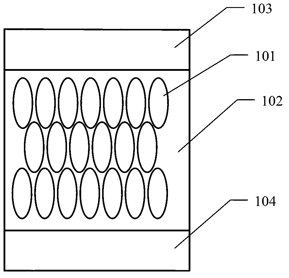
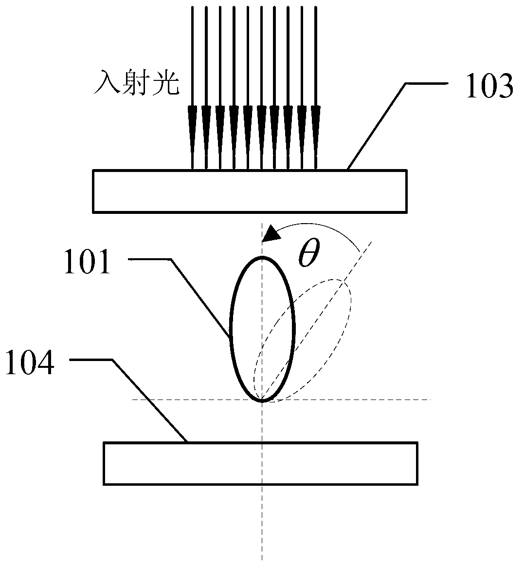
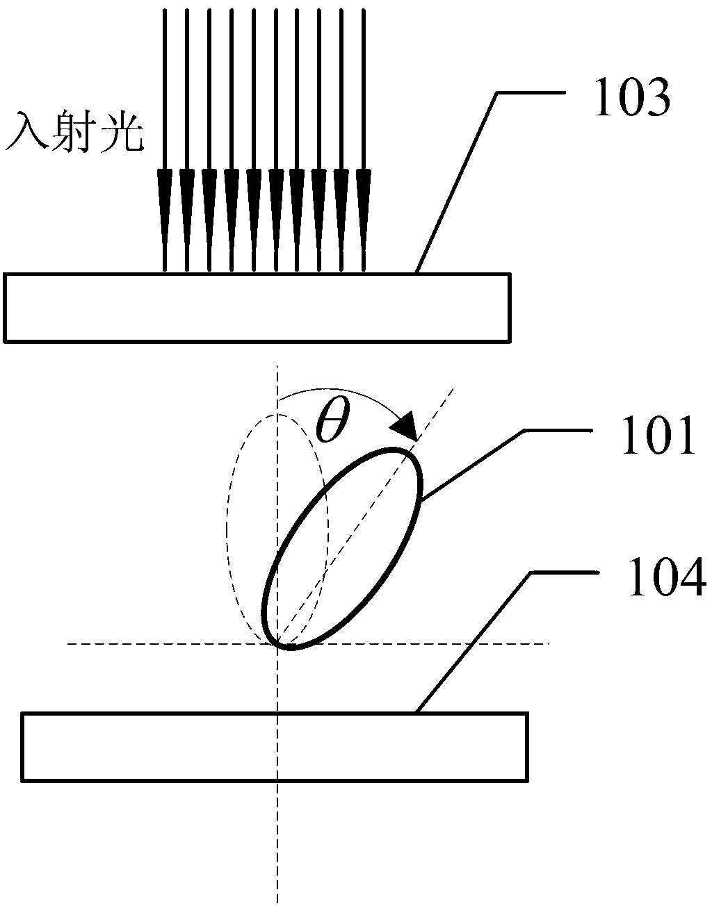
[0047] figure 1 is a schematic structural view of the display device described in the embodiment of the present invention, as shown in figure 1 , a display device provided by an embodiment of the present invention, comprising: an upper substrate 103, a lower substrate 104, and a solvent 102 between them, and also includes: The ellipsoid 101 and the ellipsoid 101 has electromagnetic properties;

[0048] The ellipsoid 101 is a nano-scale or sub-micron-scale micro ellipsoid, and the cross-section of the axis of the ellipsoid is elliptical; the reflected light wavelength of the photonic crystal varies with the distance between the upper substrate 103 and the lower substrate 104 The intensity of the applied electric field or the applied magnetic field changes; the solvent 102 acts to lubricate t...


PUM


Abstract

The invention discloses a display device which comprises an upper substrate, a lower substrate, a solvent between the upper substrate and the lower substrate and elliptic balls, wherein the elliptic balls are located between the upper substrate and the lower substrate and used for forming photonic crystals, and have electromagnetic properties. According to the display device, elliptic nanometer or submicron order balls form the photonic crystals, a light refraction coefficient is changed, light in different colors is reflected, and a colored image is displayed. Problems that an electronic paper display device based on spherical micro-balls can only display a black-and-white image or a colored image which is single in color, poorer in effect, long in response time and high in price, and a colored film of a liquid crystal display device causes optical loss in the prior art are solved.

Description

technical field [0001] The present invention relates to the field of display technology, in particular to a display device and a manufacturing method thereof. Background technique [0002] With the development of electronic paper display technology, display devices based on electronic paper technology are developing towards brighter colors, ultra-thin and energy-saving. [0003] Electronic paper display devices generally include: an upper substrate (silica gel sheet or glass substrate) and a lower substrate (silica gel sheet or glass substrate), and a liquid crystal layer or a microsphere layer between the upper substrate and the lower substrate; wherein, the upper The substrate includes a common electrode, and the lower substrate includes: a thin film transistor TFT, a pixel electrode and a reflective layer; the pixel electrode forms a variable electric field between the upper substrate and the lower substrate according to the signal received by the TFT from the data line, ...

Claims


Application Information

Patent Timeline
IPC IPC(8): G02F1/19G02F1/169
CPCG02F1/09G02F2202/32G02B26/007G02B1/005G02F1/0121G02F1/0126G02F1/0063G02F1/169G02F1/094G02F2202/01G02F1/133516G02F1/1533G02F1/133514G02F1/1339G02F1/172G09G3/344G02F1/161G02F1/1336G02F2001/1678G09G3/2003G02F1/133616G02F1/0305H01B13/0026
Inventor 梁魁袁剑峰林承武
Owner BOE TECH GRP CO LTD
Why Eureka
Try Eureka